Gesamtbetrag:
zzgl. Mwst.
Hardware Manual - phyBOARD-Mira i.MX 6 (L-843e.A1)
Table of Contents
Preface
As a member of PHYTEC's new phyBOARD® product family the phyBOARD‑Mira i.MX 6 is one of a series of PHYTEC System on Modules (SBCs) that offer off-the-shelf solutions for a huge variety of industrial applications. The new phyBOARD® product family consists of a series of extremely compact embedded control engines featuring various processing performance classes. All phyBOARDs are rated for industry, cost-optimized, and offer long-term availability. The phyBOARD‑Mira i.MX 6 is one of currently six industrial-grade carrier boards that are suitable for series production and that have been realized in accordance with Phytec's new SBCplus concept. It is an excellent example of this concept.
SBCplus Concept
The SBCplus concept was developed to meet fine differences in customer requirements with little development effort and thus greatly reduce the time-to-market.
The core of the SBCplus concept is the SBC design library (a kind of construction set) that consists of a great number of function blocks (so-called "building blocks") which are refined constantly. The recombination of these function blocks allows for the development of a customer-specific SBC within a short time. Thus, PHYTEC is able to deliver production-ready custom Single Board Computers within a few weeks at very low costs.
The already developed SBCs, such as the phyBOARD‑Mira, each represent an intersection of different customer wishes. Because of that, all necessary interfaces are already available on the standard versions, thus, allowing them to integrate into a large number of applications without modification. For any necessary detail adjustment, extension connectors are available to enable adding of a wide variety of functions.
Cost-optimized with Direct Solder Connect (DSC) Technology
At the heart of the phyBOARD‑Mira is the phyCORE-i.MX 6 System on Module (SOM). As with other SBCs of the phyBOARD® family, the SOM can be directly soldered onto the carrier board PCB for routing signals from the SOM to applicable I/O interfaces. This optional “Direct Solder Connect” (DSC) of the SOM eliminates costly PCB to PCB connectors, thereby further reducing overall system costs, and making the phyBOARDs ideally suited for deployment into a wide range of cost-optimized and robust industrial applications.
Customized Expandability from PHYTEC
Common interface signals route to standard connector interfaces on the carrier board such as Ethernet, CAN, RS-232, and audio. Due to the easily modifiable phyBOARD design approach (see "SBCplus concept"), these plug-and-play interfaces can be readily adapted in customer-specific variants according to end system requirements.
Some signals from the processor populating the SOM also extend to the expansion, and A/V connectors of the phyBOARD‑Mira. This provides for customized expandability according to end-user requirements. Thus expandability is made easy by available plug-and-play expansion modules from PHYTEC.
- HDMI and LVDS/Parallel Displays
- Power Supply, with a broad voltage range
- Industrial I/O (including WLAN)
- Home-Control Board (WiFi, KNX/EIB, I/O)
- M2M Board (GPS, GSM, I/O's)
- Debug Adapter
The default orientation of the expansion bus connectors is parallel and on the top side of the carrier board PCB. However, in custom configurations, the connectors can be mounted on the PCB's underside. Connectors in perpendicular orientation can also populate the top or underside of the PCB. This enables maximum flexibility for the orientation of expansion modules on the phyBOARD‑Mira, as well as the integration of the system into various end application physical envelopes and form factors.
Easy Integration of Display and Touch
The phyBOARD and its expansion modules enable easy connection of parallel or LVDS-based displays, as well as resistive or capacitive touch screens.
OEM Implementation
Implementation of an OEM-able SBC subassembly as the "core" of your embedded design allows you to focus on hardware peripherals and firmware without expending resources to "re-invent" microcontroller circuitry. Furthermore, much of the value of the phyBOARD® SBC lies in its layout and test.
Software Support
Production-ready Board Support Packages (BSPs) and Design Services for our hardware will further reduce your development time and risk and allow you to focus on your product expertise.
Ordering Information
Ordering numbers
phyBOARD‑Mira i.MX 6 Development Kit: KPB-01501-xxx
phyBOARD‑Mira i.MX 6 SBC: PB-01501-xxx
Product Specific Information and Technical Support
In order to receive product-specific information on changes and updates in the best way also in the future, we recommend registering at:
http://www.phytec.de/de/leistungen/entwicklungsunterstuetzung.html
or
http://www.phytec.eu/europe/oem-integration/evaluation-start-up.html
For technical support and additional information concerning your product, please visit the support section of our website which provides product-specific information, such as errata sheets, application notes, FAQs, etc.
https://www.phytec.de/produkte/single-board-computer/phyboard-mira-imx6/#downloads/
Other Products and Development Support
Aside from the new phyBOARD® family, PHYTEC supports a variety of 8-/16- and 32-bit controllers in two ways:
- as the basis for Rapid Development Kits which serve as a reference and evaluation platform
- as insert-ready, fully functional OEM modules, which can be embedded directly into the user’s peripheral hardware design.
Take advantage of PHYTEC products to shorten time-to-market, reduce development costs, and avoid substantial design issues and risks. With this new innovative full system solution, you will be able to bring your new ideas to market in the most timely and cost-efficient manner.
For more information go to:
http://www.phytec.de/support/ueberblick/
or
http://www.phytec.eu/support/ueberblick/
Declaration of Electro Magnetic Conformity of the PHYTEC phyCORE®‑Mira i.MX 6 
PHYTEC System on Module (henceforth products) are designed for installation in electrical appliances or as dedicated Evaluation Boards (i.e.: for use as a test and prototype platform for hardware/software development) in laboratory environments.
Warning
PHYTEC products lacking protective enclosures are subject to damage by ESD and, therefore, must be unpacked, handled, or operated in environments in which sufficient precautionary measures have been taken with respect to ESD dangers. Only appropriately trained personnel such as qualified electricians, technicians, and engineers should handle and/or operate these products. Moreover, PHYTEC products should not be operated without protection circuitry if connections to the product's pin header rows are longer than 3 m.
PHYTEC products fulfill the norms of the European Union’s Directive for Electro Magnetic Conformity in accordance with the descriptions and rules of usage indicated in this hardware manual (particularly with respect to the pin header row connectors, power connector, and serial interface to a host-PC).
Tip
Implementation of PHYTEC products into target devices, as well as user modifications and extensions of PHYTEC products, is subject to renewed establishment of conformity to and certification of Electro Magnetic Directives. Users should ensure conformity following any modifications to a product as well as the implementation of a product into target systems.
Product Change Management and Information Regarding Parts Populated on the SOM / SBC
With the purchase of a PHYTEC SOM / SBC, you will, in addition to our hardware and software possibilities, receive free obsolescence maintenance service for the hardware we provide. Our PCM (Product Change Management) team of developers is continuously processing all incoming PCNs (Product Change Notifications) from vendors and distributors concerning parts that are used in our products. Possible impacts on the functionality of our products due to changes in functionality or obsolesce of certain parts are constantly being evaluated in order to take the right measures either in purchasing decisions or within our hardware/software design.
Our general philosophy here is: We will never discontinue a product as long as there is a demand for it.
To fulfill this, we have established a set of methods to fulfill our philosophy:
Avoidance strategies:
- Avoid changes by evaluating the longevity of parts during the design-in phase.
- Ensure the availability of equivalent second source parts.
- Stay in close contact with part vendors to keep up with roadmap strategies.
Change management in the rare event of an obsolete and non-replaceable part:
- Ensure long-term availability by stocking parts through last-time buy management according to product forecasts.
- Offer long-term frame contracts to customers.
Change management in cases of functional changes:
- Avoid impacts on product functionality by choosing equivalent replacement parts.
- Avoid impacts on product functionality by compensating for changes through hardware redesign or backward-compatible software maintenance.
- Provide early change notifications concerning functional, relevant changes to our products.
We refrain from providing detailed part-specific information within this manual, which can be subject to continuous changes, due to part maintenance for our products.
In order to receive reliable, up-to-date, and detailed information concerning parts used for our product, please contact our support team through the contact information given within this manual.
PHYTEC Documentation
PHYTEC will provide a variety of hardware and software documentation for all of our products. This includes any or all of the following:
- QS Guide: A short guide on how to set up and boot a phyCORE board along with brief information on building a BSP, the device tree, and accessing peripherals.
- Hardware Manual: A detailed description of the System on Module and accompanying carrier board.
- Yocto Guide: A comprehensive guide for the Yocto version the phyCORE uses. This guide contains an overview of Yocto; introducing, installing, and customizing the PHYTEC BSP; how to work with programs like Poky and Bitbake; and much more.
- BSP Manual: A manual specific to the BSP version of the phyCORE. Information such as how to build the BSP, booting, updating software, device tree, and accessing peripherals can be found here.
- Development Environment Guide: This guide shows how to work with the Virtual Machine (VM) Host PHYTEC has developed and prepared to run various Development Environments. There are detailed step-by-step instructions for Eclipse and Qt Creator, which are included in the VM. There are instructions for running demo projects for these programs on a phyCORE product as well. Information on how to build a Linux host PC yourself is also a part of this guide.
- Pin Muxing Table: phyCORE SOMs have an accompanying pin table (in Excel format). This table will show the complete default signal path, from processor to carrier board. The default device tree muxing option will also be included. This gives a developer all the information needed in one location to make muxing changes and design options when developing a specialized carrier board or adapting a PHYTEC phyCORE SOM to an application.
On top of these standard manuals and guides, PHYTEC will also provide Product Change Notifications, Application Notes, and Technical Notes. These will be done on a case-by-case basis. Most of the documentation can be found on the applicable download page of our products.
Tip
After finishing the Quickstart Guide, we recommend working through the Development Environment Guide. This will give you a comprehensive overview of the features and functions of both the SOM and carrier board.
Conventions, Abbreviations, and Acronyms
This hardware manual describes the PB-01501-XXX Single Board Computer (SBC) in the following referred to as phyBOARD‑Mira i.MX 6. The manual specifies the phyBOARD‑Mira i.MX 6's design and function. Precise specifications for the NXP Semiconductors i.MX 6 microcontrollers can be found in the NXP Semiconductors i.MX 6 Data Sheet and Technical Reference Manual.
Conventions
The conventions used in this manual are as follows:
- Signals that are preceded by an "n", "/", or “#” character (e.g.: nRD, /RD, or #RD), or that have a dash on top of the signal name (e.g.: RD) are designated as active low signals. That is, their active state is when they are driven low or are driving low.
- A "0" indicates a logic zero or low-level signal, while a "1" represents a logic one or high-level signal.
- The hex numbers are given for addresses of I2C devices always represent the 7 MSB of the address byte. The correct value of the LSB which depends on the desired command (read (1), or write (0)) must be added to get the complete address byte. E.g. given address in this manual 0x41 => complete address byte = 0x83 to read from the device and 0x82 to write to the device.
- Tables that describe jumper settings show the default position in bold,bluetext.
- Text in blue indicates a hyperlink within, or external to the document. Click these links to quickly jump to the applicable URL, part, chapter, table, or figure.
- Text in bold italic indicates an interaction by the user, which is defined on the screen.
- Text in italic indicates proper names of development tools and corresponding controls (windows, tabs, commands, etc.) used within the development tool, no interaction takes place.
Abbreviations and Acronyms
Many acronyms and abbreviations are used throughout this manual. Use the table below to navigate the unfamiliar terms used in this document.
Abbreviation | Definition |
A/V | Audio/Video |
BSP | Board Support Package (Software delivered with the Development Kit including an operating system (Windows, or Linux) pre-installed on the module and Development Tools) |
CB | Carrier Board, used in reference to the phyBOARD‑Mira Development Kit Carrier Board |
DFF | D flip-flop |
DSC | Direct Solder Connect |
EMB | External memory bus |
EMI | Electromagnetic Interference |
GPI | General-purpose input |
GPIO | General-purpose input and output |
GPO | General-purpose output |
IRAM | Internal RAM, the internal static RAM on the NXP Semiconductors i.MX 6 microcontroller |
J | Solder jumpers, these types of jumpers require solder equipment to remove and place |
JP | Solderless jumpers, these types of jumpers can be removed and placed by hand with no special tools |
NC | Not Connected |
NM | Not Mounted |
NS | Not Specified |
PCB | Printed circuit board |
PDI | PHYTEC Display Interface, defined to connect Phytec display adapter boards, or custom adapters |
PEB | PHYTEC Expansion Board |
PMIC | Power management IC |
PoE | Power over Ethernet |
PoP | Package on Package |
POR | Power-on reset |
RTC | Real-time clock |
SBC | Single Board Computer, used in reference to the PBA-C(D)-06 /phyBOARD‑Mira i.MX 6 |
SMT | Surface mount technology |
SOM | System on Module, used in reference to the PCM-058 /phyCORE‑i.MX 6 module |
Sx | User button Sx (e.g. S1, S2) used in reference to the available user buttons, or DIP switches on the CB |
Sx_y | Switch y of DIP switch Sx, used in reference to the DIP switch on the carrier board |
VSTBY | SOM standby voltage input |
Abbreviations and Acronyms Used in this Manual
Introduction
Hardware Overview
The phyBOARD‑Mira for phyCORE-i.MX 6 is a low-cost, feature-rich software development platform supporting the NXP Semiconductors i.MX 6 microcontroller. Moreover, due to the numerous standard interfaces the phyBOARD‑Mira i.MX 6 can serve as the bedrock for your application. At the core of the phyBOARD‑Mira is the PCM‑058/phyCORE-i.MX 6 System On Module (SOM), containing the processor, DRAM, NAND Flash, power regulation, supervision, transceivers, and other core functions required to support the i.MX 6 processor. Surrounding the SOM is the PBA‑CD‑06/phyBOARD‑Mira carrier board, adding power input, buttons, connectors, signal breakout, and Ethernet connectivity amongst other peripherals.
The PCM-058 System On Module connects to the phyBOARD‑Mira carrier board by the use of two high-density connectors. The phyBOARD‑Mira is also available with the phyCORE-i.MX 6 in a direct solder form factor (PCL-058), a connector-less, BGA style variant of the PCM‑058/phyCORE-i.MX 6 SOM. The PCL-058 SOM is directly soldered down to the phyBOARD‑Mira using Phytec's Direct Solder Connect technology. This solution offers an ultra-low-cost Single Board Computer for the i.MX 6 processor, while maintaining most of the advantages of the SOM concept.
Adding the phyCORE-i.MX 6 SOM into your own design is as simple as ordering the connector version (PCM-058) and making use of our phyCORE Carrier Board reference schematics.
Features of the phyBOARD-Mira i.MX 6
The phyBOARD‑Mira i.MX 6 supports the following features:
- Developed in accordance with PHYTEC's new SBCplus concept (Preface)
- PHYTEC’s phyCORE-i.MX 6 SOM (optionally with Direct Solder Connect (DSC))
- Pico ITX standard dimensions (100 mm × 72 mm)
- Boot from MMC or NAND Flash
- 1.2 GHz core clock frequency and up to four cores
- 2x different power supply options (5 V via 3.5 mm combicon or 12 V – 24 V through external power module)
- 1x RJ45 jack for 10/100/1000 Mbps Ethernet
1x USB host interface brought out to an upright USB Standard-A connector or at the Mini PCI Express connector[1]
- 1x USB OTG interface available at a USB Micro-AB connector, or at the expansion connector[1]
- 1x Secure Digital / Multi-Media Memory Card interface brought out to a Micro-SD connector at the backside
- 1x CAN interface at 2×5 pin header 2.54 mm
- 1x HDMI interface brought out to a standard type A connector
- 1x LVDS interface brought out to a 20-pin FFC connector at the backside and separate connector for backlight supply and control
- 1x One-touch interface at 1x4 pin header 2.54 mm
- 1x LVDS camera interfaces compatible with PHYTEC phyCAM‑S+ camera standard with I2C for camera control
- 1x PCI interface brought out to a Mini PCI Express connector, SIM-card signals are also available at the expansion connector
- 1x RS-232 or RS-485 transceiver supporting UART3 incl. handshake signals with data rates of up to 1 Mbps (2×5 pin header 2.54 mm)
- 1x Reset-Button
- 1x One multicolor LED
- 2x Audio/Video (A/V) connectors
- 1x Expansion connector with different interfaces
- RTC
Backup supply for RTC via external 2-pole pin header or with Gold cap (lasts approx. 11 ½ days)
| 1. | Caution! There is no protective circuit for the USB interfaces brought out at the expansion connector (X17), |
Block Diagram

Block Diagram of the phyBOARD‑Mira i.MX 6
View of the phyBOARD-Mira i.MX 6
")
View of the phyBOARD‑Mira i.MX 6 (top)
")
View of the phyBOARD‑Mira i.MX 6 (bottom)
Accessing the phyBOARD-Mira Features
PHYTEC phyBOARD‑Mira is fully equipped with all mechanical and electrical components necessary for a speedy and secure start-up.
Overview of the phyBOARD-Mira Peripherals
The phyBOARD‑Mira is depicted in View of the phyBOARD‑Mira i.MX 6 (top) and View of the phyBOARD‑Mira i.MX 6 (bottom). It features many different interfaces and is equipped with the components listed below. For a more detailed description of each peripheral, refer to the appropriate section listed in the applicable table. View of the phyBOARD‑Mira i.MX 6 (top)highlights the location of each peripheral for easy identification.
Connectors and Pin Headers
The table below lists all available connectors on the phyBOARD‑Mira.
Reference Designator | Description | See Section |
X1 | phyCORE‑Connector (2 x Samtec 2x70 pin) |
|
X2 | Power supply 5 V only (via 6-pole WAGO male header, or 2‑pole Phoenix Contact MINI COMBICON base strip) | Power Connectors |
X3 | CAN connector (2×5 pin header 2.54 mm pitch) | CAN Connectivity |
X4 | Ethernet 0 connector (RJ45 with speed and link LED) | Ethernet Connectivity |
X5 | USB On-The-Go connector (USB Micro-AB) | USB Connectivity |
X6 | USB host connector (USB 2.0 Standard-A) | |
X7 | PCI Express connector (Mini PCI Express) | PCIe Connectivity |
X8 | Display backlight supply and control connector (5-pole Molex) | Backlight and Display Control Connector |
X9 | Display LVDS connector(20 pin FCC connector 1 mm pitch) | LVDS Display Connectivity |
X10 | Camera phyCAM-S+ connector (8-pole Hirose Board-to-Wire Connector 1.25 mm pitch) | Camera Connectivity |
X13 | A/V connector #1 (2×8 dual-entry connector 2 mm pitch) | Audio/Video Connectors |
X14 | A/V connector #2 (2×20 dual-entry connector 2 mm pitch) | |
X17 | Expansion connector (2×30 socket connector 2 mm pitch) | Expansion Connector |
X21 | Touch connector (1x4 pin header 2.54 mm pitch) | Touch Screen Connectivity |
X22 | Secure Digital / Multi-Media Card (Micro-slot) | Secure Digital Memory Card / Multimedia Card |
X23 | RS‑232 with RTS and CTS, or RS-485 (UART3 2×5 pin header 2.54 mm pitch) | UART Connectivity |
X28 | HDMI connector (Typ-A) | HDMI Connectivity |
X29 | Backup voltage connector (1x2 pin header 2.54 mm pitch) | VBAT, RTC, and X29 |
phyBOARD‑Mira Connectors and Pin Headers
Warning
Ensure that all module connections do not exceed their expressed maximum voltage or current. Maximum signal input values are indicated in the corresponding controller User's Manual/Data Sheets. As damage from improper connections varies according to use and application, the user must take appropriate safety measures to ensure that the module connections are protected from overloading through connected peripherals.
LEDs
The phyBOARD‑Mira is populated with three LEDs to indicate the status of the USB VBUS voltages, as well as of the power supply voltage. The fourth LED is a user-programmable RGB-LED. View of the phyBOARD‑Mira i.MX 6 (top) shows the location of the LEDs. Their function is listed in the table below.
LED | Color | Description | See Section |
D2 | red | 3.3 V voltage generation of the phyBOARD‑Mira | Power LED |
D6 | RGB | User-programmable RGB-LED | Multicolor (RGB) LED |
D13 | green | Indicates the presence of VBUS at the USB host interface | USB Connectivity |
D14 | green | Indicates the presence of VBUS at the USB OTG interface |
phyBOARD‑Mira LEDs Descriptions
Switches
The phyBOARD-Mira is populated with two switches, one to reset the phyBOARD‑Mira and another to configure the boot sequence. View of the phyBOARD‑Mira i.MX 6 (top) shows the location of the switches. Their function is listed in the table below.
Switch | Description | See Section |
S1 | Reset Button | System Reset Button |
S2 | Boot Switch | Boot Mode |
phyBOARD-Mira Switches Description
Jumpers
The phyBOARD-Mira comes pre-configured with one removable jumper (JP) and several solder jumpers (J). The jumpers allow flexible configuring of a limited number of features for the development purposes of the user.
Warning
Due to the small footprint of the solder jumpers (J), we do not recommend manual jumper modifications. This might also render the warranty invalid. Because of that only the removable jumper is described in this section. For information on the solder jumpers, see Soldering Jumpers or contact our sales team if you need jumper configurations different from the default configuration.
The function of the removable jumper on the phyBOARD‑Mira is shown below. More detailed information can be found in the appropriate section. View of the phyBOARD‑Mira i.MX 6 (top) shows the location of jumper JP2.
Jumper | Description | See Section |
JP2 | CAN Termination |
phyBOARD-Mira Jumper Description
Note
Detailed descriptions of the assembled connectors, jumpers, and switches can be found in the following sections.
Functional Components on the phyBOARD-Mira SBC
This section describes the functional components of the phyBOARD‑Mira. Each subsection details a particular connector/interface and associated jumpers for configuring that interface.
Power Supply
Warning
Do not change modules or jumper settings while the phyBOARD‑Mira is supplied with power!
Power Connectors (X2)
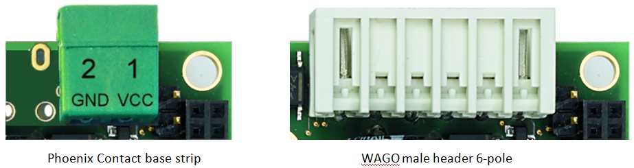
The phyBOARD‑Mira is available with two different power supply connectors. Depending on your order you will find one of the following connectors on your SBC:
- a 2-pole Phoenix Contact MINI COMBICON base strip 3.5 mm connector (X2) suitable for a single 5 V supply voltage, or
- a 6-pole WAGO male header (X2) to attach the Power Module for phyBOARDs (PEB‑POW‑01) which provides connectivity for 12 V – 24 V
The required current load capacity for all power supply solutions depends on the specific configuration of the phyCORE mounted on the phyBOARD-Mira, the particular interfaces enabled while executing software, as well as whether an optional expansion board is connected to the carrier board.
Power Supply Connectors (X2), Backup Voltage Connector (X29)
Phoenix Contact 2-pole MINI COMBICON Base Strip (X2)
The permissible input voltage is +5 V DC if your SBC is equipped with a 2-pole Phoenix Contact MINI COMBICON base strip. A 5 V adapter with a minimum supply of 1.5 A is recommended to supply the board via the 2-pole base strip. Power Supply Connectors(X2), Backup Voltage Connector (X29) and the following table show the pin assignment.
Pin | Signal | Description |
1 | VCC5V_IN | +5 V power supply |
2 | GND | Ground |
Pin Assignment of the 2-pole Phoenix Contact MINI COMBICON Base Strip at X2
WAGO 6-pole Male Header (X2)
If a WAGO 6-pole male header is mounted on your board (Power Supply Connectors (X2), Backup Voltage Connector (X29)) your board is prepared to connect to a phyBOARD Power Module (PEB‑POW‑01), or a custom power supply circuitry. The ordering number of the mating connector from WAGO is:
EAN 4045454120610
The use of the 6-pole connector has the following advantages:
- A higher and wider operational range of the input voltage
- External scaling potential to optimize the electrical output current, by use of customized power modules that match the requirements
- 5 V, 3.3 V, and backlight power supply
Pin assignment of the 6–pole WAGO connector:
Pin | Signal | Description |
1 | VCC5V_IN | +5 V power supply |
2 | GND | Ground |
3 | VCC3V3_PMOD | +3.3 V power supply |
4 | VCC_BL | Backlight power supply (input voltage of power module) |
5 | PMOD_PWRGOOD | Power good signal (connected to reset nRESET_IN) |
6 | nPMOD_PWRFAIL | Power fail signal |
Pin Assignment of the 6-pole WAGO Connector at X2
A detailed description of the Power Module for phyBOARDs can be found in the Application Guide for phyBOARD Expansion Boards (L-793e).
Power LED D2
The red LED D2 next to expansion connector X17 (View of the phyBOARD‑Mira i.MX 6 (top)) indicates the presence of the 3.3 V supply voltage generated from the 5 V input voltage.
VBAT, RTC, and X29
The phyBOARD-Mira features an external RTC at U12 (View of the phyBOARD‑Mira i.MX 6 (top)) in addition to the RTC of the Power Management IC mounted on the phyCORE‑i.MX 6 module. It is used for real-time or time-driven applications. To back up the RTC, a Gold cap (C90) (View of the phyBOARD‑Mira i.MX 6 (top)) is placed on the phyBOARD-Mira. Alternatively, the 2-pole pin header X29 can be used to connect an external battery (max. 3.6 V) to VBAT to feed in the backup voltage.
Power Supply Connectors(X2), Backup Voltage Connector (X29) and the following table show the pin assignment of X29.
Pin | Signal | Description |
1 | VBAT | Backup Battery voltage |
2 | GND | Ground |
Pinout of the 2-pole pin header X29
The backup voltage source (either Gold cap at C90, or external battery via X29) supplies the external RTC at U12. It can also be connected to the backup voltage pin VBAT (A5) of the phyCORE‑i.MX 6 via resistor R117[2]to supply some critical registers and the RTC of the Power Management IC on the SOM when the primary system power, VCC5V_IN, is removed. The backup supply for only the RTC (U12) lasts approximately 11½ days.
| 2. | Resistor R117 is not mounted in the standard configuration of the phyBOARD‑Mira. |
UART Connectivity (X17 and X23)
The i.MX 6 SOM supports up to 5 so-called UART units. On the phyBOARD‑Mira TTL level signals of UART1 and UART2 (the standard console) are routed to expansion connector X17. UART3 is available at pin header connector X23 at RS-232 level, or optionally at RS‑485 level[3].
Note
The Evaluation Board (PEB-EVAL-01) delivered with the kit plugs into the expansion connector and allows easy use of the standard console (UART2) which is required for debugging. Please find additional information on the Evaluation Board in the Application Guide for phyBOARD Expansion Boards (L‑793e).
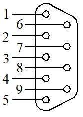
Further information on the expansion connector can be found in Expansion Connector. Pin header connector X23 is located next to the Ethernet connector (RS-232 or RS‑485 Interface Connector X23) and provides the UART3 signals of the i.MX 6 at RS-232, or RS‑485 level. The serial interface is intended to be used as data terminal equipment (DTE) and allows for a 5-wire connection including the signals RTS and CTS for hardware flow control. The table below shows the signal mapping of the RS-232 and RS-485 level signals at connector X23.
RS-232 or RS‑485 Interface Connector X23
Pin Assignment of RS-232 /RS‑485 Interface Connector X23
An adapter cable is included in the phyBOARD‑Mira i.MX 6 Kit to facilitate the use of the UART3 interface. The following figure shows the signal mapping of the adapter.
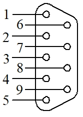
RS-232 / RS-485 Connector Signal Mapping
| 3. | The standard kit comes with an RS-232transceiver installed. |
Ethernet Connectivity (X4)
The Ethernet 0 interface of the phyBOARD‑Mira is accessible at the RJ45 connector X4.
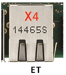
Ethernet Interface at Connectors X4
The standard phyBOARD‑Mira is equipped with an RJ45 connector supporting a 10/100Base-T network connection. Optionally, it can be ordered with phyCORE‑i.MX 6 module configured for also 1000 Mbps Ethernet and a different RJ45 connector allowing to use the phyBOARD‑Mira in a 10/100/1000Base-T network[4]. The LEDs for LINK (green) and SPEED (yellow) indications are integrated into the connector. The Ethernet transceiver supports Auto MDI-X, eliminating the need for the consideration of a direct-connect LAN or a cross-over path cable. They detect the TX and RX pins of the connected device and automatically configure the PHY TX and RX pins accordingly.
| 4. | Please contact our sales team for more information. |
USB Connectivity (X5 and X6)
The phyBOARD-Mira provides one USB host and one USB OTG interface.
USB1 is accessible at connector X5 (USB Micro-AB) and is configured as USB OTG. USB OTG devices are capable of initiating a session, controlling the connection, and exchanging host and peripheral roles with each other. This interface is compliant with USB revision 2.0. USB2 is accessible at connector X6 (USB Standard-A) and is configured as a USB host.
Both connectors are on the top side of the phyBOARD-Mira and located next to each other (Components Supporting the USB Interfaces).
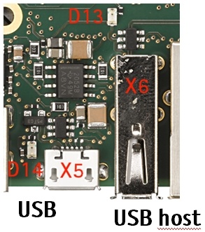
Components Supporting the USB Interfaces
LED D14 displays the status of X_USB1_VBUS and LED D13 the status of X_USB2_VBUS. Numerous jumpers configure the USB interfaces according to your needs. Please refer to Soldering Jumpersfor more information.
USB Connectivity
Rerouting the USB Interfaces to Other Connectors (J5, J6, J9, and J10)
For later expansion boards the USB1 OTG interface can be routed to the expansion connector[1] (X17). Moreover, the USB2 host interface can be routed to the Mini PCI Express connector[1] (X7). The following table shows all possible configurations.
Mode | J5 | J6 |
USB1 at USB-OTG connector X5 | 1+2 | 1+2 |
USB1 at expansion connector X17 | 2+3 | 2+3 |
USB1 (USB OTG) Routing Configuration
Mode | J9 | J10 |
USB2 at USB-A connector X6 | 1+2 | 1+2 |
USB2 at Mini PCIe connector X7 | 2+3 | 2+3 |
USB2 (USB host) Routing Configuration
| 1. | Caution! There is no protective circuit for the USB interfaces brought out at the expansion connector (X17), |
Configuring the OTG Operating Mode (R10)
Resistor R10 configures the OTG operating mode. By default, this resistor is not mounted. This leaves the USB_OTG_ID pin floating and configures the OTG interface as a slave, or according to the configuration of the connected USB device. Mounting a 10 k resistor connects the X_USB_OTG_ID pin to GND, forcing the OTG interface into host mode.
Numerous jumpers allow the USB interfaces to be configured according to your needs. Please refer to Soldering Jumpersfor more information.
CAN Connectivity (X3, JP2)
The Controller Area Network (CAN) bus offers a low-bandwidth, prioritized message fieldbus for serial communication between microcontrollers. The Flexible Controller Area Network (FLEXCAN) module of the iMX 6 implements the CAN protocol according to the CAN 2.0B protocol specification. The first interface (FLEXCAN1) of the Flexible Controller Area Network is accessible at connector X3 (2×5 pin header, 2.54 mm pitch).
Jumper JP2 can be installed to add a 120 Ohm termination resistor across the CAN data lines if needed.
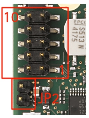
Components Supporting the CAN Interface
The table below shows the signal mapping of the CAN1 signals at connector X3.
Pin | Signal | Pin | Signal |
10 | NC | 9 | Shield |
8 | NC | 7 | NC |
6 | NC | 5 | GND |
4 | X_CANH | 3 | X_CANL |
2 | GND | 1 | NC |
Pin Assignment of CAN Connector X3
An adapter cable is included in the phyBOARD‑Mira i.MX 6 Kit to facilitate the use of the CAN interface. The following figure shows the signal mapping of the adapter.
| ||
| Pin 2 | X_CANL | |
| Pin 3 | GND | |
| Pin 5 | Shield | |
| Pin 6 | GND | |
| Pin 7 | X_CANH | |
CAN Connector Signal Mapping
As an alternative option the TTL level signals of FLEXCAN1 can be also routed to expansion port X17. Depending on the muxing options a second CAN interface (FLEXCAN2) is available at expansion port X17.
CAN Connectivity
Rerouting the CAN Interface (R110 and R111)
The first CAN interface (FLEXCAN1) can be routed to expansion connector X17. The signals are located at pin 47 (X_FLEXCAN1_TX) and pin 48 (X_FLEXCAN1_RX) of X17. The following table shows the possible configurations for FLEXCAN1.
Mode | J30 | J31 | U2 |
FLEXCAN1 at pin header X3 | n.m. | n.m. | m. |
FLEXCAN1 at expansion connector X17 (TTL level)[5] | 2+3 | 1+2 | n.m. |
Configurations for CAN Interface
| 5. | The standard kit comes with the CAN transceiver installed at U2. |
Second CAN Interface at X17
For later expansion boards the second CAN interface (FLEXCAN2) is also available at the expansion connector X17 (Expansion Connector (X17)). Usage of FLEXCAN2 at X17 requires changing of the pin muxing and additional software development.
Secure Digital Memory Card / Multimedia Card (X22)
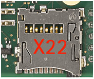
SD/MM Card Interface at Connector X22 (backside)
The phyBOARD‑Mira provides a standard microSDHC card slot at X22 for connection to SD/MMC interface cards. It allows easy and convenient connection to peripheral devices like SD and MMC cards. Power to the SD interface is supplied by inserting the appropriate card into the MMC/SD connector, which features card detection, a lock mechanism, and a smooth extraction function by Push-in/-out of the card.
DIP switch S2 toggles between NAND boot and boot from SD card. In order to boot from the SD card, S2 must be switched ON (refer to Boot Mode (S2) for further information).
PCIe Connectivity (X7)
The 1-lane PCI Express interface of the phyBOARD‑Mira i.MX 6 provides PCIe Gen. 2.0 functionality which supports 5 Gbit/s operations. Furthermore, the interface is fully backward compatible with the 2.5 Gbit/s Gen. 1.1 specification. Various control signals are implemented with GPIOs[6]. The PCIe interface is brought out at the Mini PCIe connector X7 shown in the figure below.
PCIe Interface at Connector X7
The SIM/UIM[7]card signals of a connected PCIe module can be made available at expansion connector X17. Please refer to Expansion Connector for more information about the jumper settings. Soldering jumpers connect the USB host interface to the Mini PCIe connector X7 (Soldering Jumpers). The following table is a complete overview of the Mini PCI Express connector pin assignment.
Pin # | Signal Name | Signal Type | Signal Level | Description |
1 | X_ECSPI2_MOSI/PCIe_nWAKE | IN | 3.3 V | PCIe WAKE |
2 | VCC3V3 | OUT | 3.3 V | 3.3 V power supply |
3 | X_ECSPI2_SS0/PCIe_COEX1 | I/O | 3.3 V | Coexistence pins for wireless solutions |
4 | GND | - | - | Ground |
5 | X_CSI1_DATA06/PCIe_COEX2 | I/O | 3.3 V | Coexistence pins for wireless solutions |
6 | VCC1V5 | OUT | 1.5 V | 1.5 V power supply[8] |
7 | X_ECSPI2_SCLK/PCIe_nCLKREQ | IN | 3.3 V | Clock request support |
8 | X_SIM_VCC | IN | - | UIM_PWR[9] |
9 | GND | - | - | Ground |
10 | X_SIM_IO | I/O | - | UIM_DATA[9] |
11 | X_PCIe0_CLK- | OUT | DIFF | PCIe0 reference clock - |
12 | X_SIM_CLK | IN | - | UIM_CLK[9] |
13 | X_PCIe0_CLK+ | OUT | DIFF | PCIe0 reference clock + |
14 | X_SIM_RST | IN | - | UIM_RESET[9] |
15 | GND | - | - | Ground |
16 | X_SIM_VPP | IN | - | UIM_VPP[9] |
17 | RSVD3 | - | - | Not connected |
18 | GND | - | - | Ground |
19 | RSVD4 | - | - | Not connected |
20 | X_EIM_DA14/PCIe_nW_DISABLE | OUT | 3.3 V | Wireless disable signal |
21 | GND | - | - | Ground |
22 | X_ECSPI2_MISO/PCIe_nPERST | OUT | 3.3 V |
|
23 | X_PCIe_RXN | IN | DIFF | PCIe receive - |
24 | VCC3V3 | OUT | 3.3 V | 3.3 V power supply |
25 | X_PCIe_RXP | IN | DIFF | PCIe receive + |
26 | GND | - | - | Ground |
27 | GND | - | - | Ground |
28 | VCC1V5 | OUT | 1.5 V | 1.5 V power supply |
29 | GND | - | - | Ground |
30 | X_I2C1_SCL | I/O | 3.3 V | I2C1 clock |
31 | X_PCIe_TXN | OUT | DIFF | PCIe transmit - |
32 | X_I2C1_SDA | I/O | 3.3 V | I2C1 data |
33 | X_PCIe_TXP | OUT | DIFF | PCIe transmit + |
34 | GND | - | - | Ground |
35 | GND | - | - | Ground |
36 | X_USB2_DM_PCIe | I/O | DIFF | |
37 | GND | - | - | Ground |
38 | X_USB2_DP_PCIe | I/O | DIFF | |
39 | VCC3V3 | OUT | 3.3 V | 3.3 V power supply |
40 | GND | - | - | Ground |
41 | VCC3V3 | OUT | 3.3 V | 3.3 V power supply |
42 | TP6 | IN | NS | Test point for LED_WWAN |
43 | GND | - | - | Ground |
44 | TP7 | IN | NS | Test point for LED_WLAN |
45 | RSVD9 | - | - | Not connected |
46 | TP8 | IN | NS | Test point for LED_WPAN |
47 | RSVD10 | - | - | Not connected |
48 | VCC1V5 | OUT | 1.5 V | 1.5 V power supply[12] |
49 | RSVD11 | - | - | Not connected |
50 | GND | - | - | Ground |
51 | RSVD12 | - | - | Not connected |
52 | VCC3V3 | OUT | 3.3 V | 3.3 V power supply |
S1 | GNDM1 | - | - | Ground |
S2 | GNDM2 | - | - | Ground |
Mini PCI Express Connector X7
| 6. | User Identity Module (UIM) signals |
| 7. | For these pins, there is no explicit multiplexing done in the BSP and they are configured with the i.MX6's default values. No further configuration is done and must be implemented by the developer. |
| 8. | The 1.5 V voltage can be switched OFF with signal X_CSI1_DATA09/EN_VCC1V5. |
| 9. | User Identity Module (UIM) signals |
| 10. | J9 and J10 need to be set to 2+3 to route the USB2 host interface |
| 11. | Caution! There is no protective circuit for the USB |
| 12. | The 1.5 V voltage can be switched OFF |
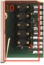
Camera Connectivity (X10)
The SOM on the phyBOARD‑Mira provides two types of camera interfaces (parallel and MIPI CSI-2).
Generally, the parallel port can be expanded on the carrier board in three ways:
- according to the phyCAM-P camera interface standard
- according to the as phyCAM-S+ camera interface standard
- as an interface for customer parallel cameras
On the phyBOARD‑Mira, the parallel Camera_0 interface is brought out as a phyCAM-S+ camera interface at connector X10 (refer to the two figures below). Information on the phyCAM-S+ standard can be found in the phyCAM-manual (L-748).
phyCAM-S+ Camera Interface on the phyBOARD‑Mira
Camera Interface (phyCAM-S+) at Connector X10
The table below shows the pinout of connector X10.
Pin # | Signal Name | Description |
1 | Camera0_L0+ | LVDS Input+ |
2 | Camera0_L0- | LVDS Input- |
3 | Camera0_RXCLK- | LVDS Clock- |
4 | I2C_SDA_CAMERA | I2C Data |
5 | I2C_SCL_CAMERA | I2C Clock |
6 | Camera0_RXCLK + | LVDS Clock+ |
7 | VCC_CAMERA0 | Power supply camera (3.3 V) |
8 | GND | Ground |
PHYTEC Camera Connector X10
HDMI Connectivity (X28)
The phyBOARD‑Mira i.MX 6 provides a High-Definition Multimedia Interface (HDMI) which is compliant with HDMI 1.4a, DVI 1.0, and HDCP 1.4. It supports a maximum pixel clock of up to 340 MHz for up to 720p at 100 Hz and 720i at 200 Hz, or 1080p at 60 Hz and 1080i/720i at 120 Hz HDTV display resolutions and a graphic display resolution of up to 2048x1536 (QXGA). Audio streams reach a sampling rate of up to 192 kHz. Please refer to the i.MX 6 Applications Processor ReferenceManual for more information.
The HDMI interface is brought out at a standard HDMI type A connector (X28) on the phyBOARD‑Mira i.MX 6 comprises the following signal groups: three pairs of data signals, one pair of clock signals, an I²C bus which is exclusively for the HDMI interface, the Consumer Electronics Control (CEC) signal, and the hotplug detect (HPD) signal. All signals are routed from the phyCORE‑Connector to the HDMI receptacle through an HDMI Transmitter Port Protection and Interface Device. This device provides ESD protection and includes level shifting to shift the I²C interface signals and the hotplug detect signal from IO voltage (VCC3V3) to 5 V. The hotplug detect signal is pulled down to ground at the output of the protection device.
Warning
Ensure that all module connections do not exceed their expressed maximum voltage or current. Maximum signal input values are indicated in the corresponding controller User's Manual/Data Sheets. As damage from improper connections varies according to use and application, the user must take appropriate safety measures to ensure that the module connections are protected from overloading through connected peripherals.
HDMI Interface Connector X28
LVDS Display Connectivity (X9)
Meanwhile, there are a few LVDS displays on the market with kind of standardized interfaces. The LVDS display connector X9 is intended to connect these displays with screen diagonals from 7” up to 12.1” at different resolutions. The display connector X9 is a 20-pole receptacle with a 1 mm pitch.
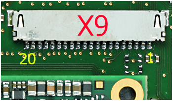
LVDS Display Connector X9
LVDS Connector (X9)
The following table is a complete overview of the LVDS display connector pin assignment.
Pin # | Signal Name | Signal Type | Signal Level | Description |
1 | VCC3V3 | OUT | 3.3 V | Power supply display[13] |
2 | VCC3V3 | OUT | 3.3 V | Power supply display[13] |
3 | X_LVDS_CONFIG1 | OUT | 3.3 V | Display configuration pin 1 |
4 | X_LVDS_CONFIG2 | OUT | 3.3 V | Display configuration pin 2 |
5 | X_LVDS0_TX0- | OUT | 3.3 V | LVDS 0 data channel 0 negative output |
6 | X_LVDS0_TX0+ | OUT | 3.3 V | LVDS 0 data channel 0 positive output |
7 | GND | - | - | Ground |
8 | X_LVDS0_TX1- | OUT | 3.3 V | LVDS 0 data channel 1 negative output |
9 | X_LVDS0_TX1+ | OUT | 3.3 V | LVDS 0 data channel 1 positive output |
10 | GND | - | - | Ground |
11 | X_LVDS0_TX2- | OUT | 3.3 V | LVDS 0 data channel 2 negative output |
12 | X_LVDS0_TX2+ | OUT | 3.3 V | LVDS 0 data channel 2 positive output |
13 | GND | - | - | Ground |
14 | X_LVDS0_CLK- | OUT | 3.3 V | LVDS 0 clock channel negative output |
15 | X_LVDS0_CLK+ | OUT | 3.3 V | LVDS 0 clock channel positive output |
16 | GND | - | - | Ground |
17 | X_LVDS_CONFIG3 | OUT | 3.3 V | Display configuration pin 3 or LVDS 0 data channel 3 negative output |
18 | X_LVDS_CONFIG4 | OUT | 3.3 V | Display configuration pin 4 or LVDS 0 data channel 3 positive output |
19 | X_LVDS_CONFIG5 | OUT | 3.3 V | Display configuration pin 5 or LVDS 0 data channel 3 negative output |
20 | X_LVDS_CONFIG6 | OUT | 3.3 V | Display configuration pin 6 or LVDS 0 data channel 3 positive output |
Pin Assignment LVDS Display Connector X9
| 13. | Provided to supply any logic on the display adapter. Max. draw 100 mA |
Various solder jumpers and resistors adapt the pin assignment to different displays. If your kit includes a display, all jumpers and resistors are preset corresponding to the display. For more detailed information about the pin assignment and how to set up the right configuration for a custom display, refer to LVDS Configurations.
Backlight and Display Control Connector (X8)
In order to support a backlight for the LVDS display, X8 provides the supply voltages and control signals necessary.

Backlight and Display Control Connector X8
The following table shows the pinout of the 1.25 mm pitch Molex PanelMateTM header.
Pin # | Signal name | Signal Type | Signal Level | Description |
1 | NC | - | - | Not connected |
2 | X_PWM1_OUT | O | 3.3 V | PWM brightness output |
3 | X_LVDS_DISP_EN | O | 3.3 V | Enable power supply display (Pull-Up R124 default nm) |
5.0 V | Enable power supply display (Pull-Up R109) | |||
4 | GND | - | - | Ground |
5 | VCC_BL | O | NS | Backlight power supply |
Display Power Connector X8 Signal Description
Touch Screen Connectivity (X13 and X21)
As many smaller applications need a touch screen as a user interface, different provisions are made to connect as well 4- wire resistive touch screens as various capacitive touch screens. A touch screen can be connected either to the dedicated touch connector X21 or to the touch signal inputs of the A/V connector X13.
The following table summarizes the different possibilities available to connect a touch screen to one of these connectors.
Connector | Touch Screen |
X21 | 4-wire resistive touch |
X13 (pins 9 – 12) | 4-wire resistive touch |
X13 (pins 15 – 16) | Capacitive touch screen with I2C interface |
Touch Screen Connectivity X13, X21
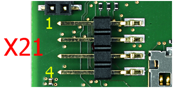
Touch Screen Connectors X21
Multicolor (RGB) LED (D6)
The phyBOARD‑Mira provides one multicolor (RGB) LED (D6) (View of the phyBOARD‑Mira i.MX 6 (top)) for user applications. The colors can be controlled with the following GPIOs.
Color | Signal | Description |
Red | X_CSI0_DAT4 | GPIO5_IO22 of the i.MX 6 |
Green | X_CSI0_DAT5 | GPIO5_IO23 of the i.MX 6 |
Blue | X_CSI0_DAT6 | GPIO5_IO24 of the i.MX 6 |
Multicolor LED Configuration
As an option, the LED can be controlled with the LED dimmer IC at U6[14]. The LED dimmer can be accessed via I2C1 at address 0X62 and dynamically controls the LED with PWM signals.
| 14. | The standard phyBOARD‑Mira kit is not equipped with an LED dimmer. |
Boot Mode (S2)
The phyBOARD‑Mira has two defined boot sequences which can be selected with DIP switch S2.
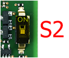
Boot Switch (S2)
Boot Mode | Description |
Boot mode 1 (S2 = OFF) | Boot from NAND |
Boot mode 2 (S2 = ON) | Boot from SD/MMC 1 |
Boot Switch Configuration (S2)
System Reset Button (S1)
The phyBOARD‑Mira is equipped with a system reset button at S1. Pressing this button will toggle the X_nRESET pin (X1D32) of the phyCORE SOM low, causing the module to reset.
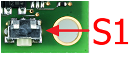
System Reset Button S1
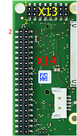
Audio/Video Connectors (X13 and X14)
The Audio/Video (A/V) connectors X13 and X14 provide an easy way to add typical A/V functions and features to the phyBOARD‑Mira. Standard interfaces such as parallel display, I2S, and I2C as well as different supply voltages are available at the two A/V female dual entry connectors. A special feature of these connectors is their connectivity from the bottom or the top.
The A/V connector is intended for use with phyBOARD Expansion Boards[15], and to add specific audio/video connectivity with custom expansion boards.
Audio/Video Connectors (X13and X14)
A/V connector X14 makes all signals for display connectivity available, while X13 provides signals for audio and touch screen connectivity, as well as an I2C bus and additional control signals.
Pin # | Signal Name | Signal Type | Signal Level | Description |
1 | GND | - | - | Ground |
2 | X_LCD_DATA16 | OUT | 3.3V | LCD Data 16 – red 0 |
3 | X_LCD_DATA17 | OUT | 3.3 V | LCD Data 17 – red 1 |
4 | X_LCD_DATA18 | OUT | 3.3 V | LCD Data 18 – red 2 |
5 | X_LCD_DATA19 | OUT | 3.3 V | LCD Data 19 – red 3 |
6 | GND | - | - | Ground |
7 | X_LCD_DATA20 | OUT | 3.3 V | LCD Data 20 – red 4 |
8 | X_LCD_DATA21 | OUT | 3.3 V | LCD Data 21 – red 5 |
9 | X_LCD_DATA22 | OUT | 3.3 V | LCD Data 22 – red 6 |
10 | X_LCD_DATA23 | OUT | 3.3 V | LCD Data 23 – red 7 |
11 | GND | - | - | Ground |
12 | X_LCD_DATA8 | OUT | 3.3 V | LCD Data 8 – green 0 |
13 | X_LCD_DATA9 | OUT | 3.3 V | LCD Data 9 – green 1 |
14 | X_LCD_DATA10 | OUT | 3.3 V | LCD Data 10 – green 2 |
15 | X_LCD_DATA11 | OUT | 3.3 V | LCD Data 11 – green 3 |
16 | GND | - | - | Ground |
17 | X_LCD_DATA12 | OUT | 3.3 V | LCD Data 12 – green 4 |
18 | X_LCD_DATA13 | OUT | 3.3 V | LCD Data 13 – green 5 |
19 | X_LCD_DATA14 | OUT | 3.3 V | LCD Data 14 – green 6 |
20 | X_LCD_DATA15 | OUT | 3.3 V | LCD Data 15 – green 7 |
21 | GND | - | - | Ground |
22 | X_LCD_DATA00 | OUT | 3.3 V | LCD Data 00 – blue 0 |
23 | X_LCD_DATA01 | OUT | 3.3 V | LCD Data 01 – blue 1 |
24 | X_LCD_DATA02 | OUT | 3.3 V | LCD Data 02 – blue 2 |
25 | X_LCD_DATA03 | OUT | 3.3 V | LCD Data 03 – blue 3 |
26 | GND | - | - | Ground |
27 | X_LCD_DATA04 | OUT | 3.3 V | LCD Data 04 – blue 4 |
28 | X_LCD_DATA05 | OUT | 3.3 V | LCD Data05 – blue 5 |
29 | X_LCD_DATA06 | OUT | 3.3 V | LCD Data 06 – blue 6 |
30 | X_LCD_DATA07 | OUT | 3.3 V | LCD Data 07 – blue 7 |
31 | GND | - | - | Ground |
32 | X_LCD_CLK | OUT | 3.3 V | LCD Pixel Clock |
33 | X_LCD_ENABLE | OUT | 3.3 V | LCD BIAS ENABLE |
34 | X_LCD_HSYNC | OUT | 3.3 V | LCD Horizontal Synchronization |
35 | X_LCD_VSYNC | OUT | 3.3 V | LCD Vertical Synchronization |
36 | GND | - | - | Ground |
37 | GND | - | - | Ground |
38 | X_PWM1_OUT | OUT | 3.3 V | Pulse Width Modulation |
39 | VCC_BL | OUT | NS | Backlight power supply[16] |
40 | VCC5V | OUT | 5.0 V | 5.0 V power supply |
PHYTEC A/V connector X13
Pin # | Signal Name | Signal Type | Signal Level | Description | |
1 | X_AUD5_TXC | I/O | 3.3 V | I²S Clock | |
2 | X_AUD5_TXFS | I/O | 3.3 V | I²S Frame | |
3 | X_AUD5_RXD | I/O | 3.3 V | I²S Analog-Digital converter (microphone) | |
4 | X_AUD5_TXD | I/O | 3.3 V | I²S Digital-Analog converter (speaker) | |
5 | X_CSI1_DATA07/AV_INT | I/O | 3.3 V | A/V interrupt, GPIO3_02[17] | |
6 | X_CSI1_DATA10/LCD_PWCTRL | OUT | 3.3 V | LCD control, GPIO3_22 | |
7 | GND | - | - | Ground | |
8 | X_nRESET | OUT | 3.3 V | Reset[18] | (J1 1+2) |
X_LCD_RESET | OUT | 3.3 V | Reset LCD | (J1 2+3) | |
9 | TS_X+ | IN | 1.8 V | Touch X+ | |
10 | TS_X- | IN | 1.8 V | Touch X- | |
11 | TS_Y+ | IN | 1.8 V | Touch Y+ | |
12 | TS_Y- | IN | 1.8 V | Touch Y- | |
13 | VCC3V3 | OUT | 3.3 V | 3.3 V power supply | |
14 | GND | - | - | Ground | |
15 | X_I2C1_SCL | I/O | 3.3 V | I2C1 Clock | |
16 | X_I2C1_SDA | I/O | 3.3 V | I2C1 Data | |
PHYTEC A/V connector X13
Jumper J1 connects either signal X_LCD_RESET or signal X_nRESET to pin 8 of X13. The following table shows the available configurations:
J1 | Description |
1+2 | X_nRESET |
2+3 | X_LCD_RESET |
A/V Jumper Configuration J1
| 15. | Please find additional information on phyBOARD Expansion Boards |
| 16. | Voltage level is not specified and depends on the |
| 17. | Note: The A/V interrupt must be enabled with signal |
| 18. | Reset signal depends on J1, please refer to |
Expansion Connector (X17)
The expansion connector X17 provides an easy way to add other functions and features to the phyBOARD‑Mira. Standard interfaces such as JTAG, UART, MMC, SPI, and I2C as well as different supply voltages and some GPIOs are available at the expansion female connector. The expansion connector is intended for use with phyBOARD Expansion Boards[15], and to add specific functions with custom expansion boards.
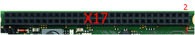
Expansion Connector (X17)
The pinout of the expansion connector is shown in the following table.
Pin # | Signal Name | Signal Type | Signal Level | Description | |
1 | VCC3V3 | OUT | 3.3 V | 3.3 V power supply | |
2 | VCC5V | OUT | 5.0 V | 5.0 V power supply | |
3 | VCC1V5 | OUT | 1.5 V | 1.5 V power supply[19] | |
4 | GND | - | - | Ground | |
5 | X_ECSPI1_SS0 | OUT | 3.3 V | SPI 1 chip select 0 | |
6 | X_ECSPI1_MOSI | OUT | 3.3 V | SPI 1 master output/slave input | |
7 | X_ECSPI1_MISO | IN | 3.3 V | SPI 1 master input/slave output | |
8 | X_ECSPI1_SCLK | OUT | 3.3 V | SPI 1 clock output | |
9 | GND | - | - | Ground | |
10 | X_UART2_RX_DATA | IN | 3.3 V | UART 2 receive data (standard debug interface) | |
11 | X_I2C1_SDA | I/O | 3.3 V | I2C 1 Data | |
12 | X_UART2_TX_DATA | OUT | 3.3 V | UART 2 transmit data (standard debug interface) | |
13 | X_I2C1_SCL | I/O | 3.3 V | I2C 1 Clock | |
14 | GND | - | - | Ground | |
15 | X_JTAG_TMS | IN | 3.3 V | JTAG Chain Test Mode Select signal | |
16 | X_JTAG_TRSTB | IN | 3.3 V | JTAG Chain Test Reset | |
17 | X_JTAG_TDI | IN | 3.3 V | JTAG Chain Test Data Input | |
18 | X_JTAG_TDO | OUT | 3.3 V | JTAG Chain Test Data Output | |
19 | GND | - | - | Ground | |
20 | X_JTAG_TCK | IN | 3.3 V | JTAG Chain Test Clock signal | |
21 | X_USB1_DP_EXP | I/O | DIFF | ||
22 | X_USB1_DM_EXP | I/O | DIFF | ||
23 | X_nRESET | OUT | 3.3 V | Reset | |
24 | GND | - | - | Ground | |
25 | X_SD3_CMD | I/O | 3.3 V | SD/MMC command | |
26 | X_SD3_DATA0 | I/O | 3.3 V | SD/MMC data 0 | |
27 | X_SD3_CLK | I/O | 3.3 V | SD/MMC clock | |
28 | X_SD3_DATA1 | I/O | 3.3 V | SD/MMC data 1 | |
29 | GND | - | - | Ground | |
30 | X_SD3_DATA2 | I/O | 3.3 V | SD/MMC data 2 | |
31 | X_CSI0_DAT11/ECSPI2_SS0 | I/O | 3.3 V | SPI2 chip select 0, UART1 RX, | |
32 | X_SD3_DATA3 | I/O | 3.3 V | SD/MMC data 3 | |
33 | X_CSI0_DAT10/ECSPI2_MISO | I/O | 3.3 V | SPI2 MISO, UART1 TX, GPIO5_28 | |
34 | GND | - | - | Ground | |
35 | X_SD3_DATA4 | I/O | 3.3 V | SD/MMC data 4, UART2 RX[22] | |
36 | X_SD3_DATA5 | I/O | 3.3 V | SD/MMC data 5, UART2 TX | |
37 | X_SATA_TXP | OUT | DIFF | SATA transmit positive | |
38 | X_SD3_DATA6 | I/O | 3.3 V | SD/MMC data 6 | |
39 | X_SATA_TXN | OUT | DIFF | SATA transmit negative | |
40 | X_SD3_DATA7 | I/O | 3.3 V | SD/MMC data 7 | |
41 | GND | - | - | Ground | |
42 | X_ECSPI2_RDY/nPMON_PWRFAIL | OUT | 3.3 V | Power fail signal | (J26 1+2) |
X_SIM_VPP | - | - | UIM_VPP | (J26 2+3) | |
43 | X_SATA_RXP | IN | DIFF | SATA receive positive | |
44 | X_CSI0_DAT8/ECSPI2_SCLK | OUT | 3.3 V | SPI 2 clock output | (J21 1+2) |
X_SIM_VCC | OUT | - | UIM VCC | (J21 2+3) | |
45 | X_SATA_RXN | IN | DIFF | SATA receive negative | |
46 | GND | - | - | Ground | |
47 | X_FLEXCAN1_TX_EXP | OUT | 3.3 V | CAN 1 transmit data[23] | (J30 2+3) |
X_PMIC_nONKEY | IN | 3.3 V | PMIC nONKEY | (J30 1+2) | |
48 | X_FLEXCAN1_RX_EXP | IN | 3.3 V | CAN 1 receive data[23] | (J31 1+2) |
49 | X_USB_OTG_OC/FLEXCAN2_TX | OUT | 3.3 V | CAN 2 transmit data | |
50 | X_USB_OTG_PWR/FLEXCAN2_RX | IN | 3.3 V | CAN 2 receive data | |
51 | GND | - | - | Ground | |
52 | X_CSI0_DAT9/ECSPI2_MOSI | OUT | 3.3 V | SPI 2 MOSI | (J25 1+2) |
X_SIM_RST | OUT | - | UIM Reset | (J25 2+3) | |
53 | X_USB1_ID | IN | 3.3 V | USB 1 identification | |
54 | X_USB1_VBUS | OUT | 5.0 V | USB 1 bus voltage | |
55 | X_USB_OTG_CHD_B | OUT | 3.3 V | USB 1 charger enable | (J23 1+2) |
X_SIM_IO | OUT | - | UIM Data | (J23 2+3) | |
56 | GND | - | - | Ground | |
57 | VCC_BL | OUT | NS | Backlight power supply[24] | |
58 | X_ECSPI2_SS1 | OUT | 3.3 V | SPI 2 chip select 1 | (J22 1+2) |
X_SIM_CLK | OUT | - | UIM Clock | (J22 2+3) | |
59 | GND | - | - | Ground | |
60 | VCC5V_IN | IN | 5.0 V | 5 V input supply voltage | |
Expansion Connector X17
Please find additional information on phyBOARD Expansion Boards The 1.5 V voltage can be switched OFF J5 and J6 need to be set to 2+3 to route the USB1 OTG interface Caution! There is no protective circuit for the USB interfaces Caution! If the UART2 signals are redirected to these pins the standard console Please refer to CAN Connectivity to make CAN 1 The voltage level is not specified and depends on the 15.
in the corresponding application guide (L-793e). 19.
with signal X_CSI1_DATA09/EN_VCC1V5. 20.
to the expansion connector (USB1 (USB OTG) Routing Configuration). 21.
brought out at the expansion connector (X17). 22.
is not available on the Evaluation Board (PEB-EVAL-01). 23.
available on the expansion connector. 24.
connected power module and the attached voltage.
CPU Core Frequency Scaling
The i.MX 6 on the phyBOARD‑Mira i.MX 6 is able to scale the clock frequency and voltage. This is used to save power when the full performance of the CPU is not needed. Scaling the frequency and the voltage is referred to as 'Dynamic Voltage and Frequency Scaling' (DVFS). The i.MX 6 BSP supports the DVFS feature. The Linux kernel provides a DVFS framework that allows each CPU core to have a min/max frequency and a governor that governs it. Depending on the i.MX 6 variant used several different frequencies are supported.
System-Level Customizing
About this Section
This section addresses advanced developers who want to design custom expansion boards or display adapters. It includes detailed information on the different interfaces and features of the phyBOARD-Mira at a system level.
System-Level Hardware Information
Soldering Jumpers
Numerous jumpers and 0 Ohm resistors configure the phyBOARD‑Mira according to your needs.
Warning
Due to the small footprint of the jumpers, we do not recommend manual jumper modifications. This might also render the warranty invalid. Please contact our sales team if you need one of the configurations described below.
The following table lists all jumpers and resistors and describes their function.
Jumper/Resistor | Description | See Section |
J1 | Selecting the reset signal at A/V connector X13 | A/V Jumper Configuration J1 |
J5, J6 | Rerouting of the USB OTG interface | |
J9, J10 | Rerouting of the USB host interface | |
J11 | Changing the I2C address of touchscreen controller U5 | |
J12 | Selecting the reset signal at Mini PCIe connector X7 | PCIe Connectivity |
J14 | Configuring rising, or falling edge strobe for the LVDS Deserializer of the phyCAM‑S+ interface | |
J17 – J20 | Adapting display connector X9 to different displays | LVDS Display Connectivity |
J21 – J23, J25, J26J | Routing of the SIM card signals to expansion connector X17 | PCIe Connectivity; Expansion Connector |
J28 | Configuring the HDMI connector's shield signals | HDMI Connectivity |
R110, R111 | Rerouting of the FLEXCAN1 interface | Rerouting the CAN Interface (R110 and R111) |
Soldering Jumpers on the phyBOARD‑Mira
I2C Connectivity
The I2C1 interface of the i.MX 6 is available at different connectors on the phyBOARD‑Mira. The following table provides a list of connectors and pins with I2C connectivity.
Connector | Location |
Mini PCIe connector X7 | pin 32 (I2C1_SDA), pin 30 (I2C1_SCL) |
phyCAM-S connector X10 | pin 4 (I2C1_SDA), pin 5 (I2C1_SCL) |
Expansion connector X17 | pin 11 (I2C1_SDA), |
A/V connector X13 | pin 16 (I2C1_SDA), |
I2C1 Connectivity
To avoid any conflicts when connecting external I2C devices to the phyBOARD‑Mira the addresses of the onboard I2C devices must be considered. The table below lists the addresses already in use and shows only the default address.
Board | Prod. No. | Device | Address used |
I2C3 | |||
phyCORE-i.MX 6 | PCM-058 | EEPROM | 0x50 |
PMIC | 0xB0, 0xB1 | ||
I2C1 | |||
phyBOARD‑Mira | PBA-C-06 | Touch controller | 0x44 |
LED dimmer | 0x62 | ||
RTC | 0x68 | ||
Mini PCIe | -[25] | ||
phyCAM-S+ | - [25] | ||
AV-Adapter HDMI | PEB-AV-01 | HDMI Core | 0x70 |
CEC Core | 0x34 | ||
AV-Adapter Display | PEB-AV-02 | GPIO Expander | 0x41 |
Evaluation Board | PEB-EVAL-01 | EEPROM | 0x56 |
M2M Board | PEB-C-01 | GPIO Expander | 0x20 |
GPIO Expander | 0x21 | ||
GPIO Expander | 0x22 | ||
I2C Addresses in Use
| 25. | Depends on the device connected |
LVDS Configurations
Various solder jumpers and resistors adapt the pin assignment to different displays. If your kit includes a display, all jumpers and resistors are preset corresponding to the display. The following table gives an overview of possible configurations. Please consider the datasheet of the display used to find the right settings.
Pin # | Signal name | J or R | Setting | Description |
3 | X_LVDS_CONFIG1 | R101[26] | if mounted | High level |
R103[26] | if mounted | Low level | ||
4 | X_LVDS_CONFIG2 | R100[26] | if mounted | High level |
R102[26] | if mounted | Low level | ||
17 | X_LVDS_CONFIG3 | J17 | 1+2 | High level |
2+3 | X_LVDS0_TX3- connected | |||
18 | X_LVDS_CONFIG4 | J18 | closed | X_LVDS0_TX3+ connected |
open | Not connected | |||
19 | X_LVDS_CONFIG5 | J19 | 1+2 | X_LVDS0_TX3- connected |
2+3 | ||||
20 | X_LVDS_CONFIG6 | J20 | 1+2 | X_LVDS0_TX3+ connected |
2+3 |
Configuration for LVDS Display Connector X9
| 26. | All configuration resistors have a value of 10 k. |
Revision History
Date | Version # | Changes in this manual |
16.10.2017 | Manual | First edition based on the AppGuide (L-806e_2) |
14.07.2022 | Manual L-843e.A1 | Moved online |