Gesamtbetrag:
zzgl. Mwst.
Camera Module Guide - phyCAM-P/phyCAM-S+ VM-012 Global Shutter (L-873e.A0)
Table of Contents
Copyrighted products are not explicitly indicated in this manual. The absence of the trademark (TM or ®) and copyright (©) symbols does not imply that a product is not protected. Additionally, registered patents and trademarks are similarly not expressly indicated in this manual.
The information in this document has been carefully checked and is considered to be entirely reliable. However, PHYTEC Messtechnik GmbH assumes no responsibility for any inaccuracies. PHYTEC Messtechnik GmbH neither gives any guarantee nor accepts any liability whatsoever for consequential damages resulting from the use of this manual or its associated product. PHYTEC Messtechnik GmbH reserves the right to alter the information contained herein without prior notification and accepts no responsibility for any damages that might result.
Additionally, PHYTEC Messtechnik GmbH offers no guarantee nor accepts any liability for damages arising from the improper usage or improper installation of the hardware or software. PHYTEC Messtechnik GmbH further reserves the right to alter the layout and/or design of the hardware without prior notification and accepts no liability for doing so.
@ Copyright 2021 PHYTEC Messtechnik GmbH, D-55129 Mainz.
Rights - including those of translation, reprint, broadcast, photomechanical or similar reproduction and storage or processing in computer systems, in whole or in part - are reserved. No reproduction may occur without the express written consent from PHYTEC Messtechnik GmbH.
| EUROPE | NORTH AMERICA | FRANCE | INDIA | CHINA |
Address: | PHYTEC Messtechnik GmbH | PHYTEC America LLC | PHYTEC France | PHYTEC Embedded Pvt. Ltd | PHYTEC Information Technology (Shenzhen) Co. Ltd. |
Ordering Information: | +49 6131 9221-32 | +1 800 278-9913 | +33 2 43 29 22 33 | +91-80-4086 7046/48 sales@phytec.in | +86-755-3395-5875 sales@phytec.cn |
Technical Support: | +49 6131 9221-31 | +1 206 780-9047 | +91-80-4086 7047 support@phytec.in | support@phytec.cn | |
Fax: | +49 6131 9221-33 | +1 206 780-9135 | +33 2 43 29 22 34 | +86-755-3395-5999 | |
Web Site: | http://phytec.in | http://www.phytec.cn |
phyCAM-P VM-012
Note
Default settings in this manual are identified using bold, blue type.
Technical Details
Specifications
- 3 MPixels – sensor (1,310,720 pixels)
- monochrome (VM-012-BW) or color (VM-012-COL)
- phyCAM-P – interface
- Framerate: 37 fps at full resolution
- Framerate: 130 fps at VGA resolution
- Global Shutter and Rolling Shutter (selectable)
- Externel Trigger and Strobe
- Secondary connector with trigger and strobe (optional)
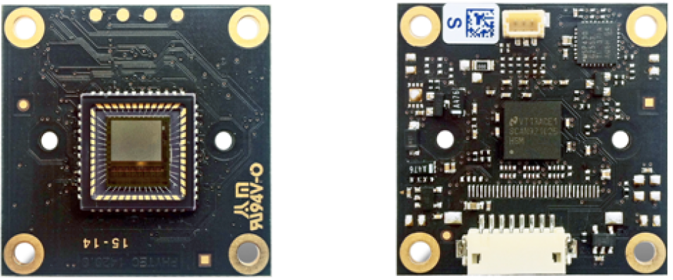
 (front / rear view)")
VM-012 (phyCAM-P) (front / rear view)
Parameters
Function | VM-012-BW[1] | VM-012-COL[1] |
Sensor | ||
Resolution | 1,3 MPixels | 1,3 MPixels |
Pixels (H x V) | 1280 x 1024 | 1280 x 1024 |
Sensor Size | 1/2" 6.18 mm x 4.95 mm | 1/2" 6.18 mm x 4.95 mm |
Pixel Size | 4.8 µm x 4.8 µm | 4.8 µm x 4.8 µm |
Color / Monochrome | monochrome | color |
Technology | CMOS | CMOS |
Image Sensor | ON Semiconductor VITA 1300 | ON Semiconductor VITA 1300 |
Scan System | progressive | progressive |
Shutter Type | global or rolling | global or rolling |
| 37 fps (full resolution) | 37 fps (full resolution) |
130 fps at VGA | 130 fps at VGA | |
Responsiveness | 4.6 V/lux.sec (at 550 nm) | 4.6 V/lux.sec (at 550 nm) |
Max. Dynamic Range | 60 dB (Rolling Shutter Mode) | 60 dB (Rolling Shutter Mode) |
High Dynamic Range | 90 dB | 90 dB |
Exposure Time | programmable | programmable |
Gain | programmable | programmable |
AEC | automatic and manual | automatic and manual |
AGC | automatic and manual | automatic and manual |
Gamma Correction | n/a | n/a |
White Balance/AWB | n/a | n/a |
Ext. Trigger / Sync. | Trigger / Strobe | Trigger / Strobe |
ROI | up to 8 | up to 8 |
Skipping | 2x2 | 2x2 |
Binning | 2x2 | 2x2 |
Mirror | n/a | n/a |
Image Processor | n/a | n/a |
LED-Light | n/a | n/a |
Special features | see Special Features | see Special Features |
Electrical Interface | ||
Video Output Type | digital | digital |
Interface | phyCAM-P | phyCAM-P |
Data Format | 8 / 10 Bit parallel | 8 / 10 Bit parallel |
Interface-Mode | Y8 / Y10 | 8 / 10 Bit RGGB (Bayer) |
Dataline-Shifting | n/a | n/a |
Camera Config. Bus | I²C | I²C |
Supply Voltage | 3.3 V | 3.3 V |
Power Consumption | 450 mW | 450 mW |
Standby Power | 26 mW | 26 mW |
Mechanical Parameters | ||
Lens Connector | without / M12 / C-CS | without / M12 / C-CS |
Lens | n/a | n/a |
Housing | n/a | n/a |
Dimensions (mm) | 34 x 34 | 34 x 34 |
Mounting | 4 x M2.5 | 4 x M2.5 |
Color (housing) | n/a | n/a |
Weight (PCB) | 5 g | 5 g |
Operating Temperature | -25...85°C | -25...85°C |
Connectors | ||
Data and Power | FFC 33 pin | FFC 33 pin |
Trigger / Sync. | FFC + JST 3 pin | FFC / JST 3 pin |
Iris | n/a | n/a |
Special functions | n/a | n/a |
VM-012 (phyCAM-P) Parameters
| 1. | n/a: not applicable. All parameters are subject to change |
Electrical Specifications
| Symbol | min. | typ. | max. | Unit |
Operating Voltage | VCAM | 3.1 | 3.3 | 3.6 | V |
Operation Current | ICAM | tbd | 450 | tbd | mA |
Input high voltage | VIH | 2 | - | VCAM +0.3 | V |
Input low voltage | VIL | -0.3 | - | 0.8 | V |
Output high voltage | VOH | 2,4 | - | - | V |
Output low voltage | VOL | - | - | 0.5 | V |
Voltage Set Resistor | R31 | - | 0 | 2 | W |
Operating Temperature[2] | TOP | -25 | - | 85 | °C |
StorageTemperature[2] | TSTG | -25 | - | 85 | °C |
| Symbol | min. | typ. | max. | Unit |
Master Clock Frequency | fMCLK | 20 | - | 62 | MHz |
Clock Duty Cycle | dutycyleMCLK | 40 | 50 | 60 | % |
Input Clock jitter | tj | - | 20 | - | ps |
MCLCK to PCLK delay | tCP | tbd. | ns | ||
PCLK to data valid | tPD | tbd. | ns | ||
PCLK to FV high | tPFH | tbd. | ns | ||
PCLK to FV low | tPFL | tbd. | ns | ||
PCLK to LV high | tPLH | tbd. | ns | ||
PCLK to LV low | tPLL | tbd. | ns | ||
I²C Frequency[3] | fI2C | - | 100 | 400 | kHz |
| 2. | The I²C master must support Clock-Stretching. |
| 3. | -30°C without the optional Trigger/Strobe-connector. |
Data Formats
Monochrome (VM-012-BW):
- Y8 : 8 bit grey scale
- Y10: 10 bit grey scale
Color (VM-012-COL):
- RGGB (Bayer-Pattern) 8 bit color depth
- RGGB (Bayer-Pattern) 10 bit color depth
Note
Any other desired lower color / grey scale resolution can be configured by using a reduced subset of the data lines. To configure this, connect only the upper data lines (MSB) to the microprocessor interface. Some microprocessors also enable dynamic configuration of the camera interface input.
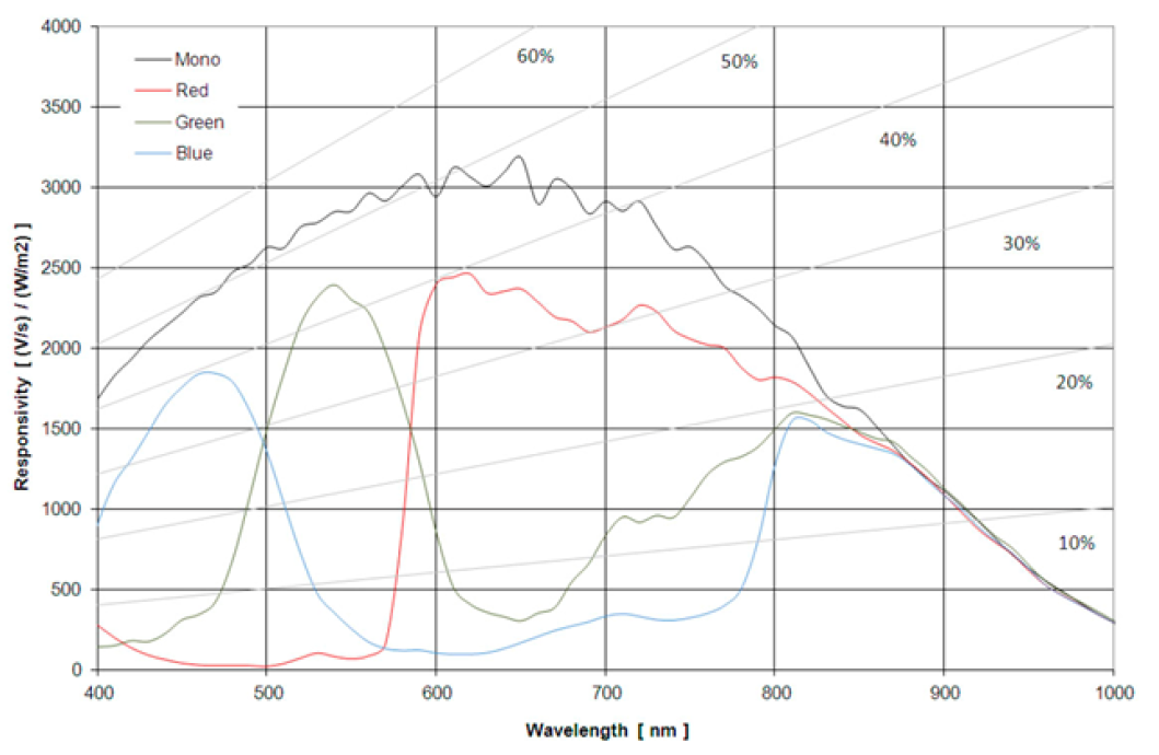
Spectral Characteristics
 Spectral Characteristics")
VM-012-BW / COL (phyCAM-P) Spectral Characteristics
Note
Please refer to the datasheet of the camera sensor for detailed characteristics.
VM-012 (phyCAM-P) Feature Pins
Signal | Pin | Function | I/O | Configuration |
CAM_CTRL1 | 7 | N.C. (not connected) | - | J11:NOMT |
I²C-Adress-Select | I | J11:1+2 | ||
Monitor Out | O | J11:2+3 | ||
CAM_CTRL2 | 30 | GND | - | J5:1+2 |
Trigger Input | I | J5:2+3 | ||
N.C. (not connected) | - | J53:NOMT | ||
CAM_RST | 3 | /Camera Reset | I | aktiv low |
CAM_OE | 32 | reserved | - | default: input without function |
CAM_MCLK | 29 | Master Clock | I | J1:2+3 |
N.C. (not connected) | - | J1:1+2 |
VM-012 (phyCAM-P) Feature Pins
Notes
Configuration: internal configuration of the camera module to activate / use this feature.
NOMT = not mounted
“not x+y” = Jumper must be set to a different setting.
In order to best meet technical requirements and cost objectives, custom configurations are available for high volume deliveries of phyCAM modules. Please consult PHYTEC for additional information.
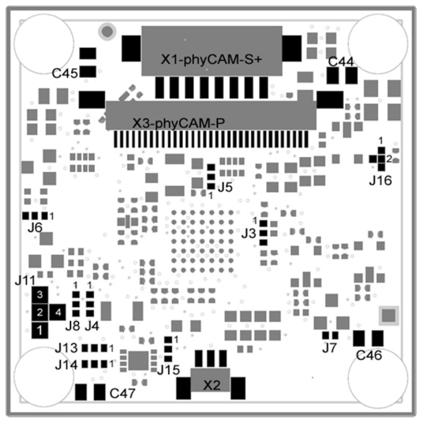
VM-012 (phyCAM-P) Jumper Map
 Jumper Map (PCB revision: PL1420.1)")
VM-012 (phyCAM-P) Jumper Map (PCB revision: PL1420.1)
VM-012 (phyCAM-P) Pixel Remapping
The pixels of the VITA 1300 image sensor are organized in kernels. This means that the readout sequence of the pixels in a line is not sequentially consecutive as one would assume from the physical position of the pixel on the sensor.
The kernel size is 8 pixels in x-direction by 1 pixel in y-direction. The kernels are organized as shown below:
![]()
VM-012 (phyCAM-P) Kernel organization in pixel array
The order in which the pixel data is output is based on the kernels and depends on the subsampling mode.
No Subsampling
The pixel sequence is different for even and odd kernels as shown below:
![]()
VM-012 (phyCAM-P) Pixel order with no subsampling
Subsampling, Monochrome Sensor
In subsampling mode, two adjacent kernels are combined to form one single kernel . This halves the number of output pixels and the even pixels are always taken. In contrast to the operating mode without subsampling, there is no difference in the pixel order of even and odd kernels. THe data order is shown below:
![]()
VM-012 (phyCAM-P) Pixel order with subsampling, monochrome sensor
Subsampling, Color Sensor
In subsampling mode two adjacent kernels are combined to form one single kernel. This halves the number of output pixels. Only the pixels 0, 1, 4, 5, 8, 9, 12, and 13 are read out. In contrast to the operating mode without subsampling, there is no difference in the pixel order of even and odd kernels. The data order is shown below:
![]()
VM-012 (phyCAM-P) Pixel order with subsampling, color sensor
Notes
The output pixels must be brought into the correct sequence by the following processing unit (usually by software) or the pixel sequence must be considered during processing.
When defining a ROI on the sensor array, the ROI margins and kernel margins must match. Ideally, the beginning of a ROI is organized in such a way that it always falls on the same kernel type ( even kernels ).
PHYTEC provides a library and GStreamer function for sorting the kernels with the development kits.
For more information, see the application note "VM-012 Remapping".
I2C Addresses
|
| Configuration | ||||
CAM_CTRL1 | J11 | J9 | J10 | Variant | ||
| 0x90 | GND | 1-2 | 2-4 | 1-2 |
|
x | x | 2-3 | ||||
0x98 | VCAM | 1-2 | 2-4 | 1-2 | ||
x | x | 1-2 | ||||
0xB0 | GND | 1-2 | 2-4 | 2-3 | ||
x | x | 2-3 | ||||
0xB8 | VCAM | 1-2 | 2-4 | 2-3 | ||
x | x | 1-2 | ||||
VM-012 (phyCAM-P) I2C Addresses
|
| Configuration |
| ||
J2 | J3 | J4 | |||
| 0xA0 | 1+2 | 1+2 | 1+2 |
|
0xA2 | 2+3 | 1+2 | 1+2 | ||
0xA4 | 1+2 | 2+3 | 1+2 | ||
0xA6 | 2+3 | 2+3 | 1+2 | ||
0xA8 | 1+2 | 1+2 | 2+3 | ||
0xAA | 2+3 | 1+2 | 2+3 | ||
0xAC | 1+2 | 2+3 | 2+3 | ||
0xAE | 2+3 | 2+3 | 2+3 | ||
VM-012 (phyCAM-P) EEPROM I2C Addresses
I²C-addresses are shown in hexadecimal, 8-bit notation. Please note that Linux possibly uses 7-bit notation. If developing with Linux notation, shift the address value one bit to the right. The table shows the write address (bit 0 = 0). To read from the device, add one to the address (bit 1 = 1).
I2C Inteface
The phyCAM interfaces have an I²C interface for communication with the components on the camera module ( i. e. sensor, EEPROM, etc.). This interface is available for both phyCAM-P and phyCAM-S(+). All registers of the camera sensor can be set by the CPU via the I²C interface according to the desired configuration. The VITA 1300 sensor on the VM-012 uses an SPI interface to access its registers.
An additional microcontroller on the VM-012 converts the I²C bus to the SPI bus. This results in some special features that must be taken into account when accessing the I²C camera sensor.
The I²C interface of the VM-012 is organized in 8-bit data blocks:
- 8-Bit device address
- 8-Bit register address
- 2 x 8-Bit data accesses
I²C access is always carried out by a 16-bit write or 16-bit read sequence. According to the I²C specification, write and read access is determined by the state of the LSB in the device address.
- write access: LSB in the device address = 0
- read access: LSB in the device address = 1
16-Bit Write Sequence
A typical byte sequence for writing into a 16 bit register of the camera sensor is shown below. The sequence is introduced by the master through the start bit, followed by the register address and two data bytes. The more significant part of the 16-bit wide data value is transmitted first followed by the less significant part.
The VM-012 delivers the acknowledgement of receipt (ACK) after each byte. All 16 data bits must be transmitted before the register is updated. The master terminates the write operation by sending the stop bit.

Writing the value 0x0284 into register 0x09 of device0x90
Note
The data value is not transferred to the specified register of the camera sensor via the SPI interface until the two data bytes have been completely transferred.
A further I²C access may only take place after termination of the internal SPI write access. Two methods can be used to comply with this specification:
Method 1
A fixed time after an I²C write access is set before a next I²C command is sent. In firmware version V0.4 of VM-012, at least 250µs must pass after an I²C write command.
Method 2
The status flag SPI_WRITE in the register VM012_STATUS (0x99) can be used to determine the end of the internal write cycle. This status flag is controlled by the internal microcontroller of the camera module.
The bit is set after a write command is detected. It is reset after the completion of the internal write cycle. The status register is described in the next section.
Note
The registers VM012-STATUS, VM012-CONTROL and VM012_FIRMWARE can be accessed any time without any waiting period. Especially this registers can be accessed while an internal write cycle is in progress.
16-Bit Read Sequence
A typical 16-bit read sequence is shown below. First, the master must send the address of the register whose contents are to be read. For this purpose, only the register address is sent to the camera module in a write sequence. The master then starts a read operation via a 16-bit value by sending a new start bit and the device address with the LSB (read identifier) set.
With the following clock pulses, the camera module sends the 16-bit register content in two data bytes. First the high byte and then the low byte are transmitted. After each 8-bit transmission, the master sends a confirmation bit (ACK). The data transmission is terminated by the master sending a No-Acknowledge bit (NACK) after the 16-bit data.

Reading the value 0x0284 from register 0x09 of device 0x90
Note
No waiting time is needed after the initial write command of a read sequence. The next read command can be sent immediately.
After the internal microcontroller of the VM-012 has received the internal I²C write command and the device address with read bit set, it takes approx. 200µs to process the command internally. The master of the I²C bus has to wait this time before he can start reading the data from the camera module.
To signal this pause, the VM-012 uses the „Clock-Stretching“ method. „Clock-Stretching“ is used only before the first data byte. The second byte is transferred immediately.
Note
The I²C-Master must support Clock-Stretching.
Internal I2C Registers
Paging
The camera sensor VITA 1300 of the VM-012 has a register map with a total of 511 registers. However many I²C routines support a register space of only 255 registers. To allow easy access to all sensor registers by all systems, the VM-012 uses paging. The I²C-address space is split into two pages of 255 registers. A page bit is used to select between lower and higher address space:
Page bit | I²C-address sent to VM-012 | Acessed register of the VITA 1300 camera sensor |
0 | 0x00 ... 0xFF | 0x000 ... 0x0FF |
1 | 0x00 ... 0xFF | 0x100 ... 0x1FF |
The sensor register accessed can be calculated by the following equation:
sensor_register = page_bit . 0x100 + I²C_register_address
The PAGE_BIT is located in the VM012_CONTROL register. A description of the sensor’s registers can be found in the VITA 1300 datasheet.
Control and Status Registers
To control the microcontroller on the camera module and to read out status information, three additional registers are mapped into the register map of the camera sensor. The I²C master can directly address the microcontroller of the VM-012 via read or write access to these registers. Three addresses are used for this which are not occupied in the address space of the VITA 1300.
Because this three addresses are not uses by the VITA 1300, this does not interfere with any functions of the sensor.
VM-012 I²C Register Address | Page-Bit[4] | Read[5] | Description |
0x97 | x | R | Firmware-Version der VM-012 |
0x98 | x | R/W | VM_012_CONTROL Register |
0x99 | x | R | VM_012_STATUS Register |
| 4. | x = don’t care |
| 5. | R = read only, R/W = read and write access |
Note
These three registers are processed directly by the microcontroller of the VM-012. They are not transmitted via SPI to the image sensor. Therefore, no delay or waiting time is needed when accessing this registers.
Register description VM012_FIRMWARE; 0x97 (151 decimal).
0x97 – VM012_FIRMWARE | |||||
Bit | Bit Name | Bit Description | DefaultHex (Dec) | LegalValues (Dec) | Read/Write |
7...0 | MINOR_REVISION | Firmware revision (minor part) | - | 0...255 | R |
15...8 | MAJOR_REVISION | Firmware revision (major part) | - | 0...255 | R |
Register description VM012_CONTROL; 0x98 (152 decimal).
0x98 – VM012_CONTROL | |||||
Bit | Bit Name | Bit Description | Default Hex (Dec) | Legal Values (Dec) | Read/Write |
| PAGE_BIT | Page selection of the image sensor register: 1 = access registers 0x100 ... 0x1FF The page bit does not change its state after a camera reset. |
|
|
|
| AUTO_SENSOR_RESET | Auto Software image sensor reset 0 = default state 1 = execute camera sensor reset cycle Writing a 1 to this bit initiates an automatic reset cycle of the image sensor. The reset signal of the sensor is asserted and the sensor’s power supply is switched off. After a delay of 100ms the sensor is powered up again and sensor reset is deasserted. |
|
|
|
| SENSOR_RESET | Image sensor reset 0 = default state 1 = image sensor reset Writing a 1 to this bit asserts the reset signal of the image sensor and the sensor’s power supply is switched off. The image sensor is kept in this state until the bit is reset to 0. Resetting this bit to 0 will power up the sensor and de-assert the sensor reset. This function can be used as a power-saving state. |
|
|
|
0x98 – VM012_CONTROL | |||||
Bit | Bit Name | Bit Description | Default Hex (Dec) | Legal Values (Dec) | Read/Write |
3...7 | RESERVED | reserved | - | - | - |
|
| Camera module reset 0 = default state 1 = execute camera module reset cycle Writing a 1 to this initiates a camera module reset cycle. A reset of the camera sensor and of the internal microcontroller is performed. After the reset cycle all registers are set to their default values. |
|
|
|
9...15 | RESERVED | reserved | - | - | - |
Register description VM012_STATUS; 0x99 (153 decimal).
0x99 – VM012_STATUS | |||||
Bit | Bit Name | Bit Description | Default Hex (Dec) | Legal Values (Dec) | Read/Write |
|
| 0 = SPI-READ idle 1 = SPI-READ in progress – only registers 0x97, 0x98 and 0x99 may be accessed. Note: If clock stretching is used, I²C read delay is inserted automatically. In this case it’s not necessary to observe this status bit. |
|
|
|
|
| 0 = SPI-WRITE idle 1 = SPI-WRITE in progress. While this bit is set, only registers 0x97, 0x98 und 0x99 may be accessed. |
|
|
|
2..15 | RESERVED | reserved | - | - | - |
VM-012 (phyCAM-P) Special Features
Windowing / ROI
As with other members of the phyCAM product family, the camera sensor of the VM-012 enables the effective image resolution to be reduced by defining readout windows (window or ROI = Region of Interest).
This also allows the amount of data generated to be optimally adapted to the requirements of the application. The frame rate can also be increased by reducing the resolution.
Depending on the operating mode, several ROIs can be defined:
- In global shutter mode, up to eight ROIs can be configured.
- In rolling shutter mode, only a single ROI is supported.
Note
If multiple ROIs are active, the pixel output order is determined by the physical position of the corresponding pixel on the sensor. This means that ROIs are masking the sensor, but they do not change the output sequence of the pixel data. Depending on the position of the multiple ROIs, the active pixels of the ROIs are nested.
Trigger
The trigger input can be configured in two ways:
- Triggered Shutter Master Mode
In this mode, the time of image acquisition is controlled by the trigger signal. A rising edge trigger input triggers image acquisition. The exposure time is controlled by the register settings of the sensor. - Pipelined Shutter Slave Mode
In this mode, the time of image acquisition and the exposure time are controlled via the trigger input. A rising edge starts the image acquisition, a falling edge stops the image acquisition.
Notes
The trigger must not be activated in the Frame Overhead Time (FOT). The First Line Indication of the monitor signal can be used to detect the beginning of the image (seeMonitor Out).
Details of the trigger function are described in the datasheet of the image sensor VITA 1300.
The trigger input is available on two connectors:
- On the CAM_CTRL2 - pin of the phyCAM-P connector if jumper J5 is set to 2+3.
- On the extension connector X2, pin 1
Pin | Dir | Function |
1 | I | TRIGGER0_IN |
2 | - | GND (signal ground) |
3 | O | MONITOR_OUT |
VM-012 (phyCAM-P) X2 – Extension Connector Pinout
Connector type: JST BM03B-SRSS-TB
Matching header: JST SHR-03V-S
Monitor Out
The MONITOR_OUT signal can be configured to output either the Monitor0 or the Monitor1 signal of the VITA 1300 image sensor:
Signal | Function | I/O | Configuration |
MONITOR_OUT | MONITOR0 | O | J7:2-3 |
MONITOR1 | O | J7:1-2 |
The MONITOR_OUT signal is available on the following connectors:
- CAM_CTRL1 - pin 7 of the phyCAM-P connector (optional, jumper setting: J11 = 2-3)
- pin 3 of the extension connector X2
The function of the monitor signal is set by the MONITOR_SELECT register of the image sensor.
Monitor configuration options (overview):
Function | Monitor0 | Monitor1 | Notes |
0 | x | x | constant low |
Integration Time | x | 1 during integration time | |
ROT[1] Indication | x | x | ‘1’ during ROT[6], ‘0’ outside |
Dual/Triple Slope Integration | x | asserted during DS/TS FOT[7] sequence | |
Start of x-Readout Indication | x | x | |
Black Line Indication | x | ‘1’ during black lines, ‘0’ outside | |
Frame Start Indication | x | ||
Start of ROT[6] Indication | x | ||
First Line Indication | x | ‘1’ during first line, ‘0’ for all others | |
Start of X-readout Indication for Black Lines | x | ||
Start of X-readout Indication for Image Lines | x |
| 6. | ROT = Row Overhead Time |
| 7. | FOT = Frame Overhead Time |
Reset
Applying a low-level (GND) at the reset input initiates a reset of the camera sensor. All registers of the camera sensor are set to their default values. The reset input should be connected to the /RESET signal of the microcontroller board. Ensure that the /RESET signal is released after power up of the sensor. MCLK should be applied to the camera before /RESET is released.
The reset signal must be held on high-level during operation of the camera module. Asserting the /RESET signal initiates a reset of the image sensor and switches the sensor supply voltages off. The sensor supply remains in off state until the /RESET signal is in active state (low).
When the /RESET signal is de-asserted (high state), access to the I²C registers of the VM-012 is possible after a delay of approx. 100 ms.
A sensor reset can also be initiated by software. For that the bit AUTO_SENSOR_RESET is set to 1. The bit is cleared automatically at the end of the sensor’s reset cycle.
The image sensor can be held in reset state permanently. During this state, the sensor’s power supply is switched off. This can be used to reduce the power consumption of the camera module.
The sensor is brought in this state by setting the bit SENSOR_RESET to 1. The sensor remains in this state until the bit is cleared by software.
When the bit is cleared, the sensor’s power supply is switched on again by the internal power controller and reset is deasserted. After approx. 100 ms the sensor can be accessed again.
Note
- After a sensor reset is performed, the contents of the sensor registers are set to default state.
- Neither read or write access of sensor registers may be performed while the image sensor is in reset state.
- The VM012 control and status registers which are mapped into the sensor’s registers can be accessed even while the sensor is performing a reset or is held in reset state.
A complete reset of the camera module can be performed by:
- Powering the camera module off and on again
- Software: Asserting bit VM-012_RESET
A complete reset of the camera module can be initiated by asserting bit VM-012_RESET. The image sensor and the internal microcontroller will perform a reset cycle. All registers are set to their default state. The bit VM-012_RESET is automatically cleared at the end of the reset cycle.
Note
Changes to the I²C address of the camera module take effect only after a complete reset of the camera module has been performed.
Output-Enable
The output enable input (pin 32) is not implemented for the VM-012 camera module. Data and control lines are always active regardless of the state of this input. The pin is connected internally to the microcontroller and has the same electrical characteristics as any other input pins.
I2C-EEPROM (optional)
As an option, a serial I²C EEPROM can be installed on the VM-012 camera module. Application-specific data (e.g. calibration data) can be stored in this EEPROM. The EEPROM is of type M24C02-RMC6TG and has a memory size of 2 kBit. The default I2C-address of the EEPROM is 0xAE.
Other addresses can be selected by setting J13, J14 and J15 (see I2C Addresses).
Data transfer rate: 100 kHz Standard Mode / 400 kHz Fast Mode
For more information please refer to the EEPROM’s datasheet.
Internal MCLK Oscillator
As an option, the camera board can be populated with a crystal oscillator. This allows the generation of the master clock MCLK on board so no external MCLK clock has to be fed into the board on pin 29 of the phyCAM-P connector.
To use the internal clock source, OZ1 must be populated and J1 must be set to 1+2 position.
SBC Kits
Single Board Computer (SBC) kits are available for various microprocessor platforms and operating systems for testing camera modules as well as application development. PHYTEC is continuously expanding the platforms supported in these kits. Please refer to www.phytec.de for the latest information on available kits. Our sales and support team is ready to assist in selection of the appropriate kits and image processing hardware.
phyCAM-S+ VM-012-xxx-LVDS
Technical Details
Specifications
- 3 MPixels – sensor (1,310,720 pixels)
- monochrome (VM-012-LVDS-BW) or
color (VM-012-LVDS-COL) - phyCAM-S+ – interface
- Framerate: 37 fps at full resolution
- Framerate: 130 fps at VGA resolution
- Global Shutter and Rolling Shutter (selectable)
- Externer Trigger and Strobe
- Secondary connector with trigger and strobe (optional)
VM-012-xxx-LVDS (phyCAM-S+)(rear / front view)
Parameters
Function | VM-012-LVDS-BW[8] | VM-012-LVDS-COL[8] |
Sensor | ||
Resolution | 1.3 MPixels | 1.3 MPixels |
Pixels (H x V) | 1280 x 1024 | 1280 x 1024 |
Sensor Size | 1/2" 6.18 mm x 4.95 mm | 1/2" 6.18 mm x 4.95 mm |
Pixel Size | 4.8 µm x 4,8 µm | 4.8 µm x 4.8 µm |
Color / Monochrome | monochrome | color |
Technology | CMOS | CMOS |
Image Sensor | ON Semiconductor VITA 1300 | ON Semiconductor VITA 1300 (NOIV2SE1300A-QDC) |
Scan System | progressive | progressive |
Shutter Type | global or rolling | global or rolling |
Fame rate (fps) | 37 fps (full resolution) | 37 fps (full resolution) |
130 fps ( VGA resolution) | 130 fps (VGA resolution) | |
Responsivity | 4,6 V/lux.sec (at 550 nm) | 4,6 V/lux.sec (at 550 nm) |
Max. Dynamic Range | 60 dB (Rolling Shutter Mode) 53 dB (Global Shutter Mode) | 60 dB (Rolling Shutter Mode) 53 dB (Global Shutter Mode) |
High Dynamic Range | 90 dB | 90 dB |
Exposure Time | programmable | programmable |
Gain | programmable | programmable |
AEC | automatic and manual | automatic and manual |
AGC | automatic and manual | automatic and manual |
Gamma Correction | n/a | n/a |
White Balance/AWB | n/a | n/a |
Ext. Trigger / Sync. | Trigger / Strobe | Trigger / Strobe |
ROI | up to 8 | up to 8 |
Skipping | 2x2 | 2x2 |
Binning | 2x2 | 2x2 |
Mirror | n/a | n/a |
Image Processor | n/a | n/a |
LED-Light | n/a | n/a |
Special features | see Special Features | see Special Features |
Electrical Interface | ||
Video Output Type | digital | digital |
Interface | phyCAM-S+ | phyCAM-S+ |
Data Format | 8 Bit serial LVDS | 8 Bit serial LVDS |
Interface-Mode | Y8 | 8 Bit RGGB (Bayer) |
Dataline-Shifting | n/a | n/a |
Camera Config. Bus | I²C | I²C |
Supply Voltage | 3.3 V | 3.3 V |
Power Consumption | 620 mW | 620 mW |
Standby Power | 85 mW | 85 mW |
Mechanical Parameters | ||
Lens Connector | without / M12 / C-CS | without / M12 / C-CS |
Lens | n/a | n/a |
Housing | n/a | n/a |
Dimensions (mm) | 34 x 34 | 34 x 34 |
Mounting | 4 x M2.5 | 4 x M2.5 |
Color (housing) | n/a | n/a |
Weight (PCB) | 5 g | 5 g |
Operating Temperature | -25...85°C | -25...85°C |
Connectors | ||
Data and Power | Hirose 8 pol. Crimp | Hirose 8 pol. Crimp |
Trigger / Sync. | JST 3 pol. Crimp | JST 3 pol. Crimp |
Iris | n/a | n/a |
Special functions | n/a | n/a |
VM-012-xxx-LVDS (phyCAM-S+) parameters
| 8. | n/a: not applicable. All parameters are subject to change |
Electrical Specifications
| Symbol | min. | typ. | max. | Unit |
Operating Voltage | VCAM | 3,0 | 3,3 | 3,6 | V |
Operating Current | ICAM | - | 200 | - | mA |
Input high voltage[9] | VIH | 2 | - | VCAM +0,3 | V |
Input low voltage[9] | VIL | -0,3 | - | 0,8 | V |
Output high voltage[9] | VOH | 2,8 | - | - | V |
Output low voltage[9] | VOL | - | - | 0,2 | V |
Operating Temperature[10] | TOP | -25 | - | 70 | °C |
Storage Temperature[10] | TSTG | -25 | - | 70 | °C |
| Symbol | min. | typ. | max. | Unit |
Master Clock Frequency | fMCLK | 20 | - | 62 | MHz |
Clock Duty Cycle | dutycycleMCLK | 40 | 50 | 60 | % |
I²C Taktrate[11] | fI2C | - | 100 | 400 | kHz |
| Symbol | Min. | Typ. | Max. | Unit |
LVDS-Serializer | |||||
Output differential voltage | IVODI | 200 | 290 | - | mV |
VOD change between complementary out states | VOS | 1.05 | 1.1 | 1.3 | mV |
Output offset voltage | DVOS | - | - | 35 | mV |
VOS change between complementary out states | IOS | - | -56 | -90 | mA |
Output current when short to GND | IOZ | -10 | ±1 | +10 | µA |
LVDS-Receiver | |||||
Input differential, positive | VIDTH+ | - | - | 100 | mV |
Input differential, negative | VIDTH– | -100 | - | - | mV |
Shunt | RSHUNT | 100 | W | ||
| 9. | CAM_SDA, CAM_SCL, I=+/-100µA |
| 10. | -30°C without the optional Trigger/Strobe-connector X2 |
| 11. | the I²C master must support Clock-Stretching |
Data Formats
monochrome (VM-012-BW-LVDS):
- Y8 : 8 bit grey scale
color (VM-012-COL-LVDS):
- RGGB (Bayer-Pattern) 8 bit color depth
Spectral Characteristics
VM-012-xxx-LVDS (phyCAM-S+) Spectral Characteristics
VM-012-xxx-LVDS (phyCAM-S+) Jumper Map
VM-012-xxx-LVDS (phyCAM-S+) Jumper Map (PCB revision: PL 1420.0)
VM-012-xxx-LVDS (phyCAM-S+) Pixel Remapping
Due to the internal structure of the VITA 1300 camera sensor, pixels are not sequentially output according to the physical arrangement on the sensor. The lines of the pixel array are rather divided into so-called kernels, which represent groups of 8 pixels each (8 pixels in x-direction per line). The kernels are organized as shown below:
![]()
VM-012-xxx-LVDS (phyCAM-S+) Kernel organization in pixel array
The order in which the pixel data is output is based on the kernels and depends on the sub-sampling mode.
No Sub-sampling
The pixel order is different in even and odd kernels as seen below.
![]()
VM-012-xxx-LVDS (phyCAM-S+) Pixel order with no sub-sampling
Sub-sampling, Monochrome Sensor
In sub-sampling mode, two adjacent kernels are combined to form one kernel. This halves the number of output pixels. The even pixels are always taken. In contrast to the operating mode without sub-sampling, there is no difference in the pixel order of even and odd kernels.
![]()
VM-012-xxx-LVDS (phyCAM-S+) Pixel order with sub-sampling, monochrome sensor
Sub-sampling, Color Sensor
In sub-sampling mode, two adjacent kernels are combined to form one kernel. This halves the number of output pixels. Two adjacent pixels are always removed and then two pixels are skipped. In contrast to the operating mode without sub-sampling, there is no difference in the pixel order of even and odd kernels.
![]()
VM-012-xxx-LVDS (phyCAM-S+) Pixel order with sub-sampling, color sensor
Notes
The output pixels must be brought into the correct sequence by the following processing unit (usually by software) or the pixel sequence must be taken into account during processing.
When defining a ROI on the sensor array, the ROI edges must coincide with the kernel boundaries. Ideally, the beginning of a ROI is organized in such a way that it always falls on the same kernel type (straight kernels).
PHYTEC provides a library and GStreamer function for sorting the kernels with the development kits. For more information, see the application note "VM-012 Remapping".
I2C Addresses
|
| Configuration |
| |
J9 | J10 | |||
| 0x90 | 2+3 | 1+2 |
|
0x98 | 1+2 | 1+2 | ||
0xB0 | 2+3 | 2+3 | ||
0xB8 | 1+2 | 2+3 | ||
VM-012-xxx-LVDS (phyCAM-S+) I2C Addresses
|
| Configuration |
| ||
J2 | J3 | J4 | |||
| 0xA0 | 1+2 | 1+2 | 1+2 |
|
0xA2 | 2+3 | 1+2 | 1+2 | ||
0xA4 | 1+2 | 2+3 | 1+2 | ||
0xA6 | 2+3 | 2+3 | 1+2 | ||
0xA8 | 1+2 | 1+2 | 2+3 | ||
0xAA | 2+3 | 1+2 | 2+3 | ||
0xAC | 1+2 | 2+3 | 2+3 | ||
0xAE | 2+3 | 2+3 | 2+3 | ||
VM-012-xxx-LVDS (phyCAM-S+) EEPROM I2C Addresses
I²C-addresses are shown in hexadecimal, 8-bit notation. Please note that Linux possibly uses a 7-bit notation. If developing with Linux notation, shift the address value one bit to the right. The table shows the write address (bit 0 = 0). To read from the device, add one to the address (bit 1 = 1).
I2C Interface Descriptions
The phyCAM interfaces have an I²C interface for communication with the components on the camera module (sensor, EEPROM, etc.). This interface is available for both phyCAM-P and phyCAM-S+. All registers of the camera sensor can be set by the CPU via the I²C interface according to the desired configuration.
The VITA 1300 sensor on the VM-012 uses an SPI interface to access its registers. An additional microcontroller on the VM-012 converts the I²C bus to the SPI bus. This results in some special features that must be taken into account when accessing the I²C camera sensor.
The I²C interface of the VM-012 is organized with a word width of 8 bits:
- 8 bit device address
- 8 bit register address
- 8 bit data accesses
Access to the I²C interface of the VM-012 is always as a 16-bit write or 16-bit read sequence. According to the I²C specification, write and read accesses are distinguished by the state of the LSB in the device address:
- Write access: LSB in the device address = 0
- Read access: LSB in the device address = 1
16-Bit Write Sequence
A typical byte sequence for writing into a 16-bit register of the camera sensor is shown below. The sequence is introduced by the master through the start bit, followed by the register address and two data bytes. The more significant part of the 16-bit wide data value is transmitted first and then the less significant part.
The VM-012 delivers the acknowledgement of receipt (ACK) after each byte. All 16 data bits must be transmitted before the register is updated. The master terminates the write operation by sending the stop bit.
Writing the value 0x0284 into register 0x09 of device 0x90
Note
The data value is not transferred to the specified register of the camera sensor via the SPI interface until the two data bytes have been completely transferred.
A further I²C access may only take place after termination of the internal SPI write access. Two methods can be used to comply with this specification:
Method 1
A fixed time after an I²C write access must elapse before the next I²C command is sent. In firmware version V0.4 of VM-012, at least 250µs must elapse after an I²C write command.
Method 2
Using the status flag SPI_WRITE in VM012_STATUS register 0x99. The status flag is managed by the microcontroller of the camera module. After recognizing a write command, this bit is set automatically and reset after completion of the SPI write process. The status register is described in 16-Bit Read Sequence.
Note
Access to the registers VM012-STATUS, VM012-CONTROL and VM012_FIRMWARE is possible without waiting times. Furthermore, access to these registers is also possible during the still active SPI write sequence.
16-Bit Read Sequence
A typical 16-bit read sequence is shown in Figure 94. First, the master must send the address of the register which content is to be read. For this purpose, only the register address is sent to the camera module in a write sequence.
The master then starts a read operation via a 16-bit value by sending a new start bit and the device address with the LSB (read identifier) set.
With the following clock pulses, the camera module sends the 16-bit register content in two data bytes. First, the high byte and then the low byte are transmitted. After each 8-bit transmission, the master sends a confirmation bit (ACK). The data transmission is terminated by the master sending a No-Acknowledge bit (NACK) after the 16-bit data.
Reading the value 0x0284 from register 0x09 of device0x90
Note
After the introductory write command within the read sequence, no waiting time must be observed. The subsequent read command can be started immediately.
After the microcontroller of the VM-012 has received the introductory I²C write command and the device address with set read bit, it usually needs approx. 200µs to process the internal SPI read command. During this time, the master must wait at the I²C interface before it can start reading the data. For this purpose, the microcontroller of the VM-012 uses the mechanism of Clock Stretching. Clock Stretching is used only once before the first data byte. The second data byte is sent immediately upon request.
Note
The I²C-Master must support Clock-Stretching.
Internal I2C Registers
Paging
The camera sensor VITA 1300 on the VM-012 has a register map with 511 registers. However, many I²C routines only support an address space of 255 registers. Therefore, the I²C address space on the VM-012 was extended by using a page bit.
page bit | I²C-address sent to VM-012 | acessed register of the |
0 | 0x00 ... 0xFF | 0x000 ... 0x0FF |
1 | 0x00 ... 0xFF | 0x100 ... 0x1FF |
The addressed register address of the camera sensor, therefore, corresponds to the register address transferred to the I²C interface plus the value of the page bit as MSB:
sensor_register = page_bit . 0x100 + I²C_register_address
Note
A description of the sensor’s registers can be found in the VITA 1300 datasheet.
Control and Status Registers
To control the microcontroller on the camera module and to read out status information, three additional registers are mapped into the register map of the camera sensor. The I²C master can directly address the microcontroller of the VM-012 via read or write access to these registers. Three addresses are used for this which are not occupied in the address space of the VITA 1300.
VM-012 | Page-Bit[12] | Read[13] | Description |
0x97 | x | R | Firmware-Version der VM-012 |
0x98 | x | R/W | VM_012_CONTROL Register |
0x99 | x | R | VM_012_STATUS Register |
| 12. | x = don’t care |
| 13. | R = read only, R/W = read and write access |
Note
These three addresses are not forwarded to the SPI interface of the camera sensor, but only evaluated in the microcontroller. They are not subject to waiting times when reading or writing on the I²C interface.
Register description VM012_FIRMWARE; 0x97 (151 decimal).
0x97 – VM012_FIRMWARE | |||||
Bit | Bit Name | Bit Description | Default | Legal | Read/Write |
7...0 | MINOR_REVISION | Firmware revision (minor part) | - | 0...255 | R |
15...8 | MAJOR_REVISION | Firmware revision (major part) | - | 0...255 | R |
Register description VM012_CONTROL; 0x98 (152 decimal).
0x98 – VM012_CONTROL | |||||
Bit | Bit Name | Bit Description | Default | Legal | Read/Write |
|
| Page selection of the image sensor register: 1 = access registers 0x100 ... 0x1FF The page bit does not change its state after a camera reset. |
|
|
|
|
| Auto Software image sensor reset 0 = default state 1 = execute camera sensor reset cycle Writing a 1 to this bit initiates an automatic reset cycle of the image sensor. The reset signal of the sensor is asserted and the sensor’s power supply is switched off. After a delay of 100ms the sensor is powered up again and sensor reset is de-asserted. |
|
|
|
|
| Image sensor reset 0 = default state 1 = image sensor reset Writing a 1 to this bit asserts the reset signal of the image sensor and the sensor’s power supply is switched off. The image sensor is kept in this state until the bit is reset to 0. Resetting this bit to 0 will power up the sensor and de-assert the sensor reset. This function can be used as a power-saving state. |
|
|
|
| 3...7 | RESERVED | reserved | - | - | - |
8 | VM-012_RESET | Camera module reset 0 = default state 1 = execute camera module reset cycle Writing a 1 to this initiates a camera module reset cycle. A reset of the camera sensor and of the internal microcontroller is performed. After the reset cycle all registers are set to their default values. | 0 | 0 ; 1 | R/W |
| 9...15 | RESERVED | reserved | - | - | - |
Register description VM012_STATUS; 0x99 (153 decimal).
0x99 – VM012_STATUS | |||||
Bit | Bit Name | Bit Description | Default | Legal | Read/Write |
|
| 0 = SPI-READ idle 1 = SPI-READ in progress – only registers 0x97, 0x98 and 0x99 may be accessed. Note: If clock stretching is used, I²C read delay is inserted automatically. In this case it’s not necessary to observe this status bit. |
|
|
|
|
| 0 = SPI-WRITE idle 1 = SPI-WRITE in progress. While this bit is set, only registers 0x97, 0x98 und 0x99 may be accessed. |
|
|
|
2..15 | RESERVED | reserved | - | - | - |
VM-012-xxx-LVDS (phyCAM-S+) Special Features
Windowing / ROI
Like other phyCAM modules, the camera sensor of the VM-012 enables the effective image resolution to be reduced by defining readout windows (window or ROI = Region of Interest). This also allows the amount of data generated to be optimally adapted to the requirements of the application. The frame rate can also be increased by reducing the resolution. Depending on the operating mode, several ROIs can be defined:
- Global Shutter Mode: up to 8 ROIs
- Rolling Shutter Mode: up to 1 ROI
Note that when using multiple ROIs, the output order of the pixels is still determined by the position of the pixels on the sensor. ROIs mask the sensor, but they do not determine the order of the pixels. If necessary, the active pixels of several ROIs are nested.Trigger
The trigger input provides the following special functions:
- Triggered Shutter Master Mode:
In this mode, the time of image acquisition is controlled by the trigger signal. A rising edge trigger input triggers image acquisition. The exposure time is controlled by the register settings of the sensor.
- Pipelined Shutter Slave Mode:
In this mode, the time of image acquisition and the exposure time are controlled via the trigger input. A rising edge starts the image acquisition, a falling edge stops the image acquisition.
Note
The trigger must not be activated in the Frame Overhead Time (FOT). The First Line Indication of the monitor signal can be used to detect the beginning of the image, see below. Details on triggering can be found in the data sheet of the camera sensor.
The trigger input is available at the extension connector X2, pin 1:
Pin | Dir | Function |
1 | I | TRIGGER0_IN |
2 | - | GND (signal ground) |
3 | O | MONITOR_OUT |
VM-012-xxx-LVDS (phyCAM-S+) X2 – Extension Connector Pinout
Connector type: JST BM03B-SRSS-TB
Matching header: JST SHR-03V-S
Monitor Out
The MONITOR_OUT signal can be configured to output either the Monitor0 or Monitor1 signal of the VITA 1300 image sensor:
Signal |
| Function | I/O | Configuration |
MONITOR_OUT | MONITOR0 | O | J7:2-3 | |
MONITOR1 | O | J7:1-2 |
The MONITOR_OUT signal is available on pin 3 of the extension connector X2. The function of the signal can be set in the register MONITOR_SELECT of the sensor.
Monitor configuration options[14] (overview):
Function | Monitor0 | Monitor1 | Notes |
0 | x | x | constant low |
Integration Time | x | 1 during integration time | |
ROT Indication | x | x | ‘1’ during ROT, ‘0’ outside |
Dual/Triple Slope Integration | x | asserted during DS/TS FOT sequence | |
Start of x-Readout Indication | x | x | |
Black Line Indication | x | ‘1’ during black lines, ‘0’ outside | |
Frame Start Indication | x | ||
Start of ROT Indication | x | ||
First Line Indication | x | ‘1’ during first line, ‘0’ for all others | |
Start of X-readout Indication for Black Lines | x | ||
Start of X-readout Indication for Image Lines | x |
| 14. | ROT = Row Overhead Time, FOT = Frame Overhead Time |
Reset
When the supply voltage is applied, a reset cycle of the camera sensor is triggered. After the internal reset cycle has been performed, I²C access to the VM-012 registers is possible after approx. 100 ms.
A sensor reset can also be triggered by software. For this purpose, the AUTO_SENSOR_RESET bit is set to 1. The bit is automatically reset at the end of the sensor reset cycle.
The image sensor can be permanently reset by software, whereby the power supply of the sensor is switched off. This can be used, for example, to reduce the power consumption of the camera module.
This state can be achieved by setting the SENSOR_RESET bit to 1. The sensor remains in this state until the bit is reset to 0. Then, the supply voltage of the image sensor is switched on again and the reset is deactivated. After approx. 100 ms, access to the sensor is possible again.
Notes
- After a sensor reset, all registers of the image sensor are set to their default values.
- Do not execute any register accesses to the image sensor while the sensor is in reset state.
- The control and status registers displayed in the register map can also be accessed during a sensor reset.
A complete reset of the camera module can be triggered by :
- Switching the operating voltage of the camera module off and on
- Software by activating bit VM-012_RESET
The complete reset can be triggered by setting bit VM-012_RESET. Then the image sensor and the internal microcontroller perform a reset. All registers are reset to their default values. Bit VM-012_RESET is reset automatically.
I2C-EEPROM
The camera module VM-012 can optionally be equipped with an EEPROM. Application-specific data (e.g. calibration data) can be stored in this EEPROM. The EEPROM is of type M24C02-RMC6TG and has a memory size of 2 kBit. The default I2C address is 0xAE. Alternative addresses can be set via jumpers (see I2C Addresses). Data transmission rate: 100 kHz Standard Mode / 400 kHz Fast Mode.
Further information can be found in the data sheet of the EEPROM.
Internal MCLK Oscillator
If required, it is possible to equip an oscillator on the camera board camera module. This can generate the Masterclock MCLK for the camera sensor. It is then no longer necessary to feed the MCLK clock via pins 3/6 of the phyCAM-S connector. To use the internal master clock, OZ1 must be equipped and jumper J1 must be set to 1+2.
SBC Kits
Single Board Computer (SBC) kits are available for various microprocessor platforms and operating systems for testing camera modules as well as application development. PHYTEC is continuously expanding the platforms supported in these kits. Please refer to www.phytec.de for the latest information on available kits. Our sales and support team is ready to assist in selection of the appropriate kits and image processing hardware.
Revision History
Date | Version # | Changes in this manual |
01.03.2021 | Manual L-873e.A0 | New Release |
Copyrighted products are not explicitly indicated in this manual. The absence of the trademark (TM or ®) and copyright (©) symbols does not imply that a product is not protected. Additionally, registered patents and trademarks are similarly not expressly indicated in this manual.
The information in this document has been carefully checked and is considered to be entirely reliable. However, PHYTEC Messtechnik GmbH assumes no responsibility for any inaccuracies. PHYTEC Messtechnik GmbH neither gives any guarantee nor accepts any liability whatsoever for consequential damages resulting from the use of this manual or its associated product. PHYTEC Messtechnik GmbH reserves the right to alter the information contained herein without prior notification and accepts no responsibility for any damages that might result.
Additionally, PHYTEC Messtechnik GmbH offers no guarantee nor accepts any liability for damages arising from the improper usage or improper installation of the hardware or software. PHYTEC Messtechnik GmbH further reserves the right to alter the layout and/or design of the hardware without prior notification and accepts no liability for doing so.
@ Copyright 2021 PHYTEC Messtechnik GmbH, D-55129 Mainz.
Rights - including those of translation, reprint, broadcast, photomechanical or similar reproduction and storage or processing in computer systems, in whole or in part - are reserved. No reproduction may occur without the express written consent from PHYTEC Messtechnik GmbH.
| EUROPE | NORTH AMERICA | FRANCE | INDIA | CHINA |
Address: | PHYTEC Messtechnik GmbH | PHYTEC America LLC | PHYTEC France | PHYTEC Embedded Pvt. Ltd | PHYTEC Information Technology (Shenzhen) Co. Ltd. |
Ordering Information: | +49 6131 9221-32 | +1 800 278-9913 | +33 2 43 29 22 33 | +91-80-4086 7046/48 sales@phytec.in | +86-755-3395-5875 sales@phytec.cn |
Technical Support: | +49 6131 9221-31 | +1 206 780-9047 | +91-80-4086 7047 support@phytec.in | support@phytec.cn | |
Fax: | +49 6131 9221-33 | +1 206 780-9135 | +33 2 43 29 22 34 | +86-755-3395-5999 | |
Web Site: | http://phytec.in | http://www.phytec.cn |
phyCAM-P VM-012
Note
Default settings in this manual are identified using bold, blue type.
Technical Details
Specifications
- 3 MPixels – sensor (1,310,720 pixels)
- monochrome (VM-012-BW) or color (VM-012-COL)
- phyCAM-P – interface
- Framerate: 37 fps at full resolution
- Framerate: 130 fps at VGA resolution
- Global Shutter and Rolling Shutter (selectable)
- Externel Trigger and Strobe
- Secondary connector with trigger and strobe (optional)
VM-012 (phyCAM-P) (front / rear view)
Parameters
Function | VM-012-BW[1] | VM-012-COL[1] |
Sensor | ||
Resolution | 1,3 MPixels | 1,3 MPixels |
Pixels (H x V) | 1280 x 1024 | 1280 x 1024 |
Sensor Size | 1/2" 6.18 mm x 4.95 mm | 1/2" 6.18 mm x 4.95 mm |
Pixel Size | 4.8 µm x 4.8 µm | 4.8 µm x 4.8 µm |
Color / Monochrome | monochrome | color |
Technology | CMOS | CMOS |
Image Sensor | ON Semiconductor VITA 1300 | ON Semiconductor VITA 1300 |
Scan System | progressive | progressive |
Shutter Type | global or rolling | global or rolling |
| 37 fps (full resolution) | 37 fps (full resolution) |
130 fps at VGA | 130 fps at VGA | |
Responsiveness | 4.6 V/lux.sec (at 550 nm) | 4.6 V/lux.sec (at 550 nm) |
Max. Dynamic Range | 60 dB (Rolling Shutter Mode) | 60 dB (Rolling Shutter Mode) |
High Dynamic Range | 90 dB | 90 dB |
Exposure Time | programmable | programmable |
Gain | programmable | programmable |
AEC | automatic and manual | automatic and manual |
AGC | automatic and manual | automatic and manual |
Gamma Correction | n/a | n/a |
White Balance/AWB | n/a | n/a |
Ext. Trigger / Sync. | Trigger / Strobe | Trigger / Strobe |
ROI | up to 8 | up to 8 |
Skipping | 2x2 | 2x2 |
Binning | 2x2 | 2x2 |
Mirror | n/a | n/a |
Image Processor | n/a | n/a |
LED-Light | n/a | n/a |
Special features | see Special Features | see Special Features |
Electrical Interface | ||
Video Output Type | digital | digital |
Interface | phyCAM-P | phyCAM-P |
Data Format | 8 / 10 Bit parallel | 8 / 10 Bit parallel |
Interface-Mode | Y8 / Y10 | 8 / 10 Bit RGGB (Bayer) |
Dataline-Shifting | n/a | n/a |
Camera Config. Bus | I²C | I²C |
Supply Voltage | 3.3 V | 3.3 V |
Power Consumption | 450 mW | 450 mW |
Standby Power | 26 mW | 26 mW |
Mechanical Parameters | ||
Lens Connector | without / M12 / C-CS | without / M12 / C-CS |
Lens | n/a | n/a |
Housing | n/a | n/a |
Dimensions (mm) | 34 x 34 | 34 x 34 |
Mounting | 4 x M2.5 | 4 x M2.5 |
Color (housing) | n/a | n/a |
Weight (PCB) | 5 g | 5 g |
Operating Temperature | -25...85°C | -25...85°C |
Connectors | ||
Data and Power | FFC 33 pin | FFC 33 pin |
Trigger / Sync. | FFC + JST 3 pin | FFC / JST 3 pin |
Iris | n/a | n/a |
Special functions | n/a | n/a |
VM-012 (phyCAM-P) Parameters
| 1. | n/a: not applicable. All parameters are subject to change |
Electrical Specifications
| Symbol | min. | typ. | max. | Unit |
Operating Voltage | VCAM | 3.1 | 3.3 | 3.6 | V |
Operation Current | ICAM | tbd | 450 | tbd | mA |
Input high voltage | VIH | 2 | - | VCAM +0.3 | V |
Input low voltage | VIL | -0.3 | - | 0.8 | V |
Output high voltage | VOH | 2,4 | - | - | V |
Output low voltage | VOL | - | - | 0.5 | V |
Voltage Set Resistor | R31 | - | 0 | 2 | W |
Operating Temperature[2] | TOP | -25 | - | 85 | °C |
StorageTemperature[2] | TSTG | -25 | - | 85 | °C |
| Symbol | min. | typ. | max. | Unit |
Master Clock Frequency | fMCLK | 20 | - | 62 | MHz |
Clock Duty Cycle | dutycyleMCLK | 40 | 50 | 60 | % |
Input Clock jitter | tj | - | 20 | - | ps |
MCLCK to PCLK delay | tCP | tbd. | ns | ||
PCLK to data valid | tPD | tbd. | ns | ||
PCLK to FV high | tPFH | tbd. | ns | ||
PCLK to FV low | tPFL | tbd. | ns | ||
PCLK to LV high | tPLH | tbd. | ns | ||
PCLK to LV low | tPLL | tbd. | ns | ||
I²C Frequency[3] | fI2C | - | 100 | 400 | kHz |
| 2. | The I²C master must support Clock-Stretching. |
| 3. | -30°C without the optional Trigger/Strobe-connector. |
Data Formats
Monochrome (VM-012-BW):
- Y8 : 8 bit grey scale
- Y10: 10 bit grey scale
Color (VM-012-COL):
- RGGB (Bayer-Pattern) 8 bit color depth
- RGGB (Bayer-Pattern) 10 bit color depth
Note
Any other desired lower color / grey scale resolution can be configured by using a reduced subset of the data lines. To configure this, connect only the upper data lines (MSB) to the microprocessor interface. Some microprocessors also enable dynamic configuration of the camera interface input.
Spectral Characteristics
VM-012-BW / COL (phyCAM-P) Spectral Characteristics
Note
Please refer to the datasheet of the camera sensor for detailed characteristics.
VM-012 (phyCAM-P) Feature Pins
Signal | Pin | Function | I/O | Configuration |
CAM_CTRL1 | 7 | N.C. (not connected) | - | J11:NOMT |
I²C-Adress-Select | I | J11:1+2 | ||
Monitor Out | O | J11:2+3 | ||
CAM_CTRL2 | 30 | GND | - | J5:1+2 |
Trigger Input | I | J5:2+3 | ||
N.C. (not connected) | - | J53:NOMT | ||
CAM_RST | 3 | /Camera Reset | I | aktiv low |
CAM_OE | 32 | reserved | - | default: input without function |
CAM_MCLK | 29 | Master Clock | I | J1:2+3 |
N.C. (not connected) | - | J1:1+2 |
VM-012 (phyCAM-P) Feature Pins
Notes
Configuration: internal configuration of the camera module to activate / use this feature.
NOMT = not mounted
“not x+y” = Jumper must be set to a different setting.
In order to best meet technical requirements and cost objectives, custom configurations are available for high volume deliveries of phyCAM modules. Please consult PHYTEC for additional information.
VM-012 (phyCAM-P) Jumper Map
VM-012 (phyCAM-P) Jumper Map (PCB revision: PL1420.1)
VM-012 (phyCAM-P) Pixel Remapping
The pixels of the VITA 1300 image sensor are organized in kernels. This means that the readout sequence of the pixels in a line is not sequentially consecutive as one would assume from the physical position of the pixel on the sensor.
The kernel size is 8 pixels in x-direction by 1 pixel in y-direction. The kernels are organized as shown below:
![]()
VM-012 (phyCAM-P) Kernel organization in pixel array
The order in which the pixel data is output is based on the kernels and depends on the subsampling mode.
No Subsampling
The pixel sequence is different for even and odd kernels as shown below:
![]()
VM-012 (phyCAM-P) Pixel order with no subsampling
Subsampling, Monochrome Sensor
In subsampling mode, two adjacent kernels are combined to form one single kernel . This halves the number of output pixels and the even pixels are always taken. In contrast to the operating mode without subsampling, there is no difference in the pixel order of even and odd kernels. THe data order is shown below:
![]()
VM-012 (phyCAM-P) Pixel order with subsampling, monochrome sensor
Subsampling, Color Sensor
In subsampling mode two adjacent kernels are combined to form one single kernel. This halves the number of output pixels. Only the pixels 0, 1, 4, 5, 8, 9, 12, and 13 are read out. In contrast to the operating mode without subsampling, there is no difference in the pixel order of even and odd kernels. The data order is shown below:
![]()
VM-012 (phyCAM-P) Pixel order with subsampling, color sensor
Notes
The output pixels must be brought into the correct sequence by the following processing unit (usually by software) or the pixel sequence must be considered during processing.
When defining a ROI on the sensor array, the ROI margins and kernel margins must match. Ideally, the beginning of a ROI is organized in such a way that it always falls on the same kernel type ( even kernels ).
PHYTEC provides a library and GStreamer function for sorting the kernels with the development kits.
For more information, see the application note "VM-012 Remapping".
I2C Addresses
|
| Configuration | ||||
CAM_CTRL1 | J11 | J9 | J10 | Variant | ||
| 0x90 | GND | 1-2 | 2-4 | 1-2 |
|
x | x | 2-3 | ||||
0x98 | VCAM | 1-2 | 2-4 | 1-2 | ||
x | x | 1-2 | ||||
0xB0 | GND | 1-2 | 2-4 | 2-3 | ||
x | x | 2-3 | ||||
0xB8 | VCAM | 1-2 | 2-4 | 2-3 | ||
x | x | 1-2 | ||||
VM-012 (phyCAM-P) I2C Addresses
|
| Configuration |
| ||
J2 | J3 | J4 | |||
| 0xA0 | 1+2 | 1+2 | 1+2 |
|
0xA2 | 2+3 | 1+2 | 1+2 | ||
0xA4 | 1+2 | 2+3 | 1+2 | ||
0xA6 | 2+3 | 2+3 | 1+2 | ||
0xA8 | 1+2 | 1+2 | 2+3 | ||
0xAA | 2+3 | 1+2 | 2+3 | ||
0xAC | 1+2 | 2+3 | 2+3 | ||
0xAE | 2+3 | 2+3 | 2+3 | ||
VM-012 (phyCAM-P) EEPROM I2C Addresses
I²C-addresses are shown in hexadecimal, 8-bit notation. Please note that Linux possibly uses 7-bit notation. If developing with Linux notation, shift the address value one bit to the right. The table shows the write address (bit 0 = 0). To read from the device, add one to the address (bit 1 = 1).
I2C Inteface
The phyCAM interfaces have an I²C interface for communication with the components on the camera module ( i. e. sensor, EEPROM, etc.). This interface is available for both phyCAM-P and phyCAM-S(+). All registers of the camera sensor can be set by the CPU via the I²C interface according to the desired configuration. The VITA 1300 sensor on the VM-012 uses an SPI interface to access its registers.
An additional microcontroller on the VM-012 converts the I²C bus to the SPI bus. This results in some special features that must be taken into account when accessing the I²C camera sensor.
The I²C interface of the VM-012 is organized in 8-bit data blocks:
- 8-Bit device address
- 8-Bit register address
- 2 x 8-Bit data accesses
I²C access is always carried out by a 16-bit write or 16-bit read sequence. According to the I²C specification, write and read access is determined by the state of the LSB in the device address.
- write access: LSB in the device address = 0
- read access: LSB in the device address = 1
16-Bit Write Sequence
A typical byte sequence for writing into a 16 bit register of the camera sensor is shown below. The sequence is introduced by the master through the start bit, followed by the register address and two data bytes. The more significant part of the 16-bit wide data value is transmitted first followed by the less significant part.
The VM-012 delivers the acknowledgement of receipt (ACK) after each byte. All 16 data bits must be transmitted before the register is updated. The master terminates the write operation by sending the stop bit.
Writing the value 0x0284 into register 0x09 of device0x90
Note
The data value is not transferred to the specified register of the camera sensor via the SPI interface until the two data bytes have been completely transferred.
A further I²C access may only take place after termination of the internal SPI write access. Two methods can be used to comply with this specification:
Method 1
A fixed time after an I²C write access is set before a next I²C command is sent. In firmware version V0.4 of VM-012, at least 250µs must pass after an I²C write command.
Method 2
The status flag SPI_WRITE in the register VM012_STATUS (0x99) can be used to determine the end of the internal write cycle. This status flag is controlled by the internal microcontroller of the camera module.
The bit is set after a write command is detected. It is reset after the completion of the internal write cycle. The status register is described in the next section.
Note
The registers VM012-STATUS, VM012-CONTROL and VM012_FIRMWARE can be accessed any time without any waiting period. Especially this registers can be accessed while an internal write cycle is in progress.
16-Bit Read Sequence
A typical 16-bit read sequence is shown below. First, the master must send the address of the register whose contents are to be read. For this purpose, only the register address is sent to the camera module in a write sequence. The master then starts a read operation via a 16-bit value by sending a new start bit and the device address with the LSB (read identifier) set.
With the following clock pulses, the camera module sends the 16-bit register content in two data bytes. First the high byte and then the low byte are transmitted. After each 8-bit transmission, the master sends a confirmation bit (ACK). The data transmission is terminated by the master sending a No-Acknowledge bit (NACK) after the 16-bit data.
Reading the value 0x0284 from register 0x09 of device 0x90
Note
No waiting time is needed after the initial write command of a read sequence. The next read command can be sent immediately.
After the internal microcontroller of the VM-012 has received the internal I²C write command and the device address with read bit set, it takes approx. 200µs to process the command internally. The master of the I²C bus has to wait this time before he can start reading the data from the camera module.
To signal this pause, the VM-012 uses the „Clock-Stretching“ method. „Clock-Stretching“ is used only before the first data byte. The second byte is transferred immediately.
Note
The I²C-Master must support Clock-Stretching.
Internal I2C Registers
Paging
The camera sensor VITA 1300 of the VM-012 has a register map with a total of 511 registers. However many I²C routines support a register space of only 255 registers. To allow easy access to all sensor registers by all systems, the VM-012 uses paging. The I²C-address space is split into two pages of 255 registers. A page bit is used to select between lower and higher address space:
Page bit | I²C-address sent to VM-012 | Acessed register of the VITA 1300 camera sensor |
0 | 0x00 ... 0xFF | 0x000 ... 0x0FF |
1 | 0x00 ... 0xFF | 0x100 ... 0x1FF |
The sensor register accessed can be calculated by the following equation:
sensor_register = page_bit . 0x100 + I²C_register_address
The PAGE_BIT is located in the VM012_CONTROL register. A description of the sensor’s registers can be found in the VITA 1300 datasheet.
Control and Status Registers
To control the microcontroller on the camera module and to read out status information, three additional registers are mapped into the register map of the camera sensor. The I²C master can directly address the microcontroller of the VM-012 via read or write access to these registers. Three addresses are used for this which are not occupied in the address space of the VITA 1300.
Because this three addresses are not uses by the VITA 1300, this does not interfere with any functions of the sensor.
VM-012 I²C Register Address | Page-Bit[4] | Read[5] | Description |
0x97 | x | R | Firmware-Version der VM-012 |
0x98 | x | R/W | VM_012_CONTROL Register |
0x99 | x | R | VM_012_STATUS Register |
| 4. | x = don’t care |
| 5. | R = read only, R/W = read and write access |
Note
These three registers are processed directly by the microcontroller of the VM-012. They are not transmitted via SPI to the image sensor. Therefore, no delay or waiting time is needed when accessing this registers.
Register description VM012_FIRMWARE; 0x97 (151 decimal).
0x97 – VM012_FIRMWARE | |||||
Bit | Bit Name | Bit Description | DefaultHex (Dec) | LegalValues (Dec) | Read/Write |
7...0 | MINOR_REVISION | Firmware revision (minor part) | - | 0...255 | R |
15...8 | MAJOR_REVISION | Firmware revision (major part) | - | 0...255 | R |
Register description VM012_CONTROL; 0x98 (152 decimal).
0x98 – VM012_CONTROL | |||||
Bit | Bit Name | Bit Description | Default Hex (Dec) | Legal Values (Dec) | Read/Write |
| PAGE_BIT | Page selection of the image sensor register: 1 = access registers 0x100 ... 0x1FF The page bit does not change its state after a camera reset. |
|
|
|
| AUTO_SENSOR_RESET | Auto Software image sensor reset 0 = default state 1 = execute camera sensor reset cycle Writing a 1 to this bit initiates an automatic reset cycle of the image sensor. The reset signal of the sensor is asserted and the sensor’s power supply is switched off. After a delay of 100ms the sensor is powered up again and sensor reset is deasserted. |
|
|
|
| SENSOR_RESET | Image sensor reset 0 = default state 1 = image sensor reset Writing a 1 to this bit asserts the reset signal of the image sensor and the sensor’s power supply is switched off. The image sensor is kept in this state until the bit is reset to 0. Resetting this bit to 0 will power up the sensor and de-assert the sensor reset. This function can be used as a power-saving state. |
|
|
|
0x98 – VM012_CONTROL | |||||
Bit | Bit Name | Bit Description | Default Hex (Dec) | Legal Values (Dec) | Read/Write |
3...7 | RESERVED | reserved | - | - | - |
|
| Camera module reset 0 = default state 1 = execute camera module reset cycle Writing a 1 to this initiates a camera module reset cycle. A reset of the camera sensor and of the internal microcontroller is performed. After the reset cycle all registers are set to their default values. |
|
|
|
9...15 | RESERVED | reserved | - | - | - |
Register description VM012_STATUS; 0x99 (153 decimal).
0x99 – VM012_STATUS | |||||
Bit | Bit Name | Bit Description | Default Hex (Dec) | Legal Values (Dec) | Read/Write |
|
| 0 = SPI-READ idle 1 = SPI-READ in progress – only registers 0x97, 0x98 and 0x99 may be accessed. Note: If clock stretching is used, I²C read delay is inserted automatically. In this case it’s not necessary to observe this status bit. |
|
|
|
|
| 0 = SPI-WRITE idle 1 = SPI-WRITE in progress. While this bit is set, only registers 0x97, 0x98 und 0x99 may be accessed. |
|
|
|
2..15 | RESERVED | reserved | - | - | - |
VM-012 (phyCAM-P) Special Features
Windowing / ROI
As with other members of the phyCAM product family, the camera sensor of the VM-012 enables the effective image resolution to be reduced by defining readout windows (window or ROI = Region of Interest).
This also allows the amount of data generated to be optimally adapted to the requirements of the application. The frame rate can also be increased by reducing the resolution.
Depending on the operating mode, several ROIs can be defined:
- In global shutter mode, up to eight ROIs can be configured.
- In rolling shutter mode, only a single ROI is supported.
Note
If multiple ROIs are active, the pixel output order is determined by the physical position of the corresponding pixel on the sensor. This means that ROIs are masking the sensor, but they do not change the output sequence of the pixel data. Depending on the position of the multiple ROIs, the active pixels of the ROIs are nested.
Trigger
The trigger input can be configured in two ways:
- Triggered Shutter Master Mode
In this mode, the time of image acquisition is controlled by the trigger signal. A rising edge trigger input triggers image acquisition. The exposure time is controlled by the register settings of the sensor. - Pipelined Shutter Slave Mode
In this mode, the time of image acquisition and the exposure time are controlled via the trigger input. A rising edge starts the image acquisition, a falling edge stops the image acquisition.
Notes
The trigger must not be activated in the Frame Overhead Time (FOT). The First Line Indication of the monitor signal can be used to detect the beginning of the image (seeMonitor Out).
Details of the trigger function are described in the datasheet of the image sensor VITA 1300.
The trigger input is available on two connectors:
- On the CAM_CTRL2 - pin of the phyCAM-P connector if jumper J5 is set to 2+3.
- On the extension connector X2, pin 1
Pin | Dir | Function |
1 | I | TRIGGER0_IN |
2 | - | GND (signal ground) |
3 | O | MONITOR_OUT |
VM-012 (phyCAM-P) X2 – Extension Connector Pinout
Connector type: JST BM03B-SRSS-TB
Matching header: JST SHR-03V-S
Monitor Out
The MONITOR_OUT signal can be configured to output either the Monitor0 or the Monitor1 signal of the VITA 1300 image sensor:
Signal | Function | I/O | Configuration |
MONITOR_OUT | MONITOR0 | O | J7:2-3 |
MONITOR1 | O | J7:1-2 |
The MONITOR_OUT signal is available on the following connectors:
- CAM_CTRL1 - pin 7 of the phyCAM-P connector (optional, jumper setting: J11 = 2-3)
- pin 3 of the extension connector X2
The function of the monitor signal is set by the MONITOR_SELECT register of the image sensor.
Monitor configuration options (overview):
Function | Monitor0 | Monitor1 | Notes |
0 | x | x | constant low |
Integration Time | x | 1 during integration time | |
ROT[1] Indication | x | x | ‘1’ during ROT[6], ‘0’ outside |
Dual/Triple Slope Integration | x | asserted during DS/TS FOT[7] sequence | |
Start of x-Readout Indication | x | x | |
Black Line Indication | x | ‘1’ during black lines, ‘0’ outside | |
Frame Start Indication | x | ||
Start of ROT[6] Indication | x | ||
First Line Indication | x | ‘1’ during first line, ‘0’ for all others | |
Start of X-readout Indication for Black Lines | x | ||
Start of X-readout Indication for Image Lines | x |
| 6. | ROT = Row Overhead Time |
| 7. | FOT = Frame Overhead Time |
Reset
Applying a low-level (GND) at the reset input initiates a reset of the camera sensor. All registers of the camera sensor are set to their default values. The reset input should be connected to the /RESET signal of the microcontroller board. Ensure that the /RESET signal is released after power up of the sensor. MCLK should be applied to the camera before /RESET is released.
The reset signal must be held on high-level during operation of the camera module. Asserting the /RESET signal initiates a reset of the image sensor and switches the sensor supply voltages off. The sensor supply remains in off state until the /RESET signal is in active state (low).
When the /RESET signal is de-asserted (high state), access to the I²C registers of the VM-012 is possible after a delay of approx. 100 ms.
A sensor reset can also be initiated by software. For that the bit AUTO_SENSOR_RESET is set to 1. The bit is cleared automatically at the end of the sensor’s reset cycle.
The image sensor can be held in reset state permanently. During this state, the sensor’s power supply is switched off. This can be used to reduce the power consumption of the camera module.
The sensor is brought in this state by setting the bit SENSOR_RESET to 1. The sensor remains in this state until the bit is cleared by software.
When the bit is cleared, the sensor’s power supply is switched on again by the internal power controller and reset is deasserted. After approx. 100 ms the sensor can be accessed again.
Note
- After a sensor reset is performed, the contents of the sensor registers are set to default state.
- Neither read or write access of sensor registers may be performed while the image sensor is in reset state.
- The VM012 control and status registers which are mapped into the sensor’s registers can be accessed even while the sensor is performing a reset or is held in reset state.
A complete reset of the camera module can be performed by:
- Powering the camera module off and on again
- Software: Asserting bit VM-012_RESET
A complete reset of the camera module can be initiated by asserting bit VM-012_RESET. The image sensor and the internal microcontroller will perform a reset cycle. All registers are set to their default state. The bit VM-012_RESET is automatically cleared at the end of the reset cycle.
Note
Changes to the I²C address of the camera module take effect only after a complete reset of the camera module has been performed.
Output-Enable
The output enable input (pin 32) is not implemented for the VM-012 camera module. Data and control lines are always active regardless of the state of this input. The pin is connected internally to the microcontroller and has the same electrical characteristics as any other input pins.
I2C-EEPROM (optional)
As an option, a serial I²C EEPROM can be installed on the VM-012 camera module. Application-specific data (e.g. calibration data) can be stored in this EEPROM. The EEPROM is of type M24C02-RMC6TG and has a memory size of 2 kBit. The default I2C-address of the EEPROM is 0xAE.
Other addresses can be selected by setting J13, J14 and J15 (see I2C Addresses).
Data transfer rate: 100 kHz Standard Mode / 400 kHz Fast Mode
For more information please refer to the EEPROM’s datasheet.
Internal MCLK Oscillator
As an option, the camera board can be populated with a crystal oscillator. This allows the generation of the master clock MCLK on board so no external MCLK clock has to be fed into the board on pin 29 of the phyCAM-P connector.
To use the internal clock source, OZ1 must be populated and J1 must be set to 1+2 position.
SBC Kits
Single Board Computer (SBC) kits are available for various microprocessor platforms and operating systems for testing camera modules as well as application development. PHYTEC is continuously expanding the platforms supported in these kits. Please refer to www.phytec.de for the latest information on available kits. Our sales and support team is ready to assist in selection of the appropriate kits and image processing hardware.
phyCAM-S+ VM-012-xxx-LVDS
Technical Details
Specifications
- 3 MPixels – sensor (1,310,720 pixels)
- monochrome (VM-012-LVDS-BW) or
color (VM-012-LVDS-COL) - phyCAM-S+ – interface
- Framerate: 37 fps at full resolution
- Framerate: 130 fps at VGA resolution
- Global Shutter and Rolling Shutter (selectable)
- Externer Trigger and Strobe
- Secondary connector with trigger and strobe (optional)
VM-012-xxx-LVDS (phyCAM-S+)(rear / front view)
Parameters
Function | VM-012-LVDS-BW[8] | VM-012-LVDS-COL[8] |
Sensor | ||
Resolution | 1.3 MPixels | 1.3 MPixels |
Pixels (H x V) | 1280 x 1024 | 1280 x 1024 |
Sensor Size | 1/2" 6.18 mm x 4.95 mm | 1/2" 6.18 mm x 4.95 mm |
Pixel Size | 4.8 µm x 4,8 µm | 4.8 µm x 4.8 µm |
Color / Monochrome | monochrome | color |
Technology | CMOS | CMOS |
Image Sensor | ON Semiconductor VITA 1300 | ON Semiconductor VITA 1300 (NOIV2SE1300A-QDC) |
Scan System | progressive | progressive |
Shutter Type | global or rolling | global or rolling |
Fame rate (fps) | 37 fps (full resolution) | 37 fps (full resolution) |
130 fps ( VGA resolution) | 130 fps (VGA resolution) | |
Responsivity | 4,6 V/lux.sec (at 550 nm) | 4,6 V/lux.sec (at 550 nm) |
Max. Dynamic Range | 60 dB (Rolling Shutter Mode) 53 dB (Global Shutter Mode) | 60 dB (Rolling Shutter Mode) 53 dB (Global Shutter Mode) |
High Dynamic Range | 90 dB | 90 dB |
Exposure Time | programmable | programmable |
Gain | programmable | programmable |
AEC | automatic and manual | automatic and manual |
AGC | automatic and manual | automatic and manual |
Gamma Correction | n/a | n/a |
White Balance/AWB | n/a | n/a |
Ext. Trigger / Sync. | Trigger / Strobe | Trigger / Strobe |
ROI | up to 8 | up to 8 |
Skipping | 2x2 | 2x2 |
Binning | 2x2 | 2x2 |
Mirror | n/a | n/a |
Image Processor | n/a | n/a |
LED-Light | n/a | n/a |
Special features | see Special Features | see Special Features |
Electrical Interface | ||
Video Output Type | digital | digital |
Interface | phyCAM-S+ | phyCAM-S+ |
Data Format | 8 Bit serial LVDS | 8 Bit serial LVDS |
Interface-Mode | Y8 | 8 Bit RGGB (Bayer) |
Dataline-Shifting | n/a | n/a |
Camera Config. Bus | I²C | I²C |
Supply Voltage | 3.3 V | 3.3 V |
Power Consumption | 620 mW | 620 mW |
Standby Power | 85 mW | 85 mW |
Mechanical Parameters | ||
Lens Connector | without / M12 / C-CS | without / M12 / C-CS |
Lens | n/a | n/a |
Housing | n/a | n/a |
Dimensions (mm) | 34 x 34 | 34 x 34 |
Mounting | 4 x M2.5 | 4 x M2.5 |
Color (housing) | n/a | n/a |
Weight (PCB) | 5 g | 5 g |
Operating Temperature | -25...85°C | -25...85°C |
Connectors | ||
Data and Power | Hirose 8 pol. Crimp | Hirose 8 pol. Crimp |
Trigger / Sync. | JST 3 pol. Crimp | JST 3 pol. Crimp |
Iris | n/a | n/a |
Special functions | n/a | n/a |
VM-012-xxx-LVDS (phyCAM-S+) parameters
| 8. | n/a: not applicable. All parameters are subject to change |
Electrical Specifications
| Symbol | min. | typ. | max. | Unit |
Operating Voltage | VCAM | 3,0 | 3,3 | 3,6 | V |
Operating Current | ICAM | - | 200 | - | mA |
Input high voltage[9] | VIH | 2 | - | VCAM +0,3 | V |
Input low voltage[9] | VIL | -0,3 | - | 0,8 | V |
Output high voltage[9] | VOH | 2,8 | - | - | V |
Output low voltage[9] | VOL | - | - | 0,2 | V |
Operating Temperature[10] | TOP | -25 | - | 70 | °C |
Storage Temperature[10] | TSTG | -25 | - | 70 | °C |
| Symbol | min. | typ. | max. | Unit |
Master Clock Frequency | fMCLK | 20 | - | 62 | MHz |
Clock Duty Cycle | dutycycleMCLK | 40 | 50 | 60 | % |
I²C Taktrate[11] | fI2C | - | 100 | 400 | kHz |
| Symbol | Min. | Typ. | Max. | Unit |
LVDS-Serializer | |||||
Output differential voltage | IVODI | 200 | 290 | - | mV |
VOD change between complementary out states | VOS | 1.05 | 1.1 | 1.3 | mV |
Output offset voltage | DVOS | - | - | 35 | mV |
VOS change between complementary out states | IOS | - | -56 | -90 | mA |
Output current when short to GND | IOZ | -10 | ±1 | +10 | µA |
LVDS-Receiver | |||||
Input differential, positive | VIDTH+ | - | - | 100 | mV |
Input differential, negative | VIDTH– | -100 | - | - | mV |
Shunt | RSHUNT | 100 | W | ||
| 9. | CAM_SDA, CAM_SCL, I=+/-100µA |
| 10. | -30°C without the optional Trigger/Strobe-connector X2 |
| 11. | the I²C master must support Clock-Stretching |
Data Formats
monochrome (VM-012-BW-LVDS):
- Y8 : 8 bit grey scale
color (VM-012-COL-LVDS):
- RGGB (Bayer-Pattern) 8 bit color depth
Spectral Characteristics
VM-012-xxx-LVDS (phyCAM-S+) Spectral Characteristics
VM-012-xxx-LVDS (phyCAM-S+) Jumper Map
VM-012-xxx-LVDS (phyCAM-S+) Jumper Map (PCB revision: PL 1420.0)
VM-012-xxx-LVDS (phyCAM-S+) Pixel Remapping
Due to the internal structure of the VITA 1300 camera sensor, pixels are not sequentially output according to the physical arrangement on the sensor. The lines of the pixel array are rather divided into so-called kernels, which represent groups of 8 pixels each (8 pixels in x-direction per line). The kernels are organized as shown below:
![]()
VM-012-xxx-LVDS (phyCAM-S+) Kernel organization in pixel array
The order in which the pixel data is output is based on the kernels and depends on the sub-sampling mode.
No Sub-sampling
The pixel order is different in even and odd kernels as seen below.
![]()
VM-012-xxx-LVDS (phyCAM-S+) Pixel order with no sub-sampling
Sub-sampling, Monochrome Sensor
In sub-sampling mode, two adjacent kernels are combined to form one kernel. This halves the number of output pixels. The even pixels are always taken. In contrast to the operating mode without sub-sampling, there is no difference in the pixel order of even and odd kernels.
![]()
VM-012-xxx-LVDS (phyCAM-S+) Pixel order with sub-sampling, monochrome sensor
Sub-sampling, Color Sensor
In sub-sampling mode, two adjacent kernels are combined to form one kernel. This halves the number of output pixels. Two adjacent pixels are always removed and then two pixels are skipped. In contrast to the operating mode without sub-sampling, there is no difference in the pixel order of even and odd kernels.
![]()
VM-012-xxx-LVDS (phyCAM-S+) Pixel order with sub-sampling, color sensor
Notes
The output pixels must be brought into the correct sequence by the following processing unit (usually by software) or the pixel sequence must be taken into account during processing.
When defining a ROI on the sensor array, the ROI edges must coincide with the kernel boundaries. Ideally, the beginning of a ROI is organized in such a way that it always falls on the same kernel type (straight kernels).
PHYTEC provides a library and GStreamer function for sorting the kernels with the development kits. For more information, see the application note "VM-012 Remapping".
I2C Addresses
|
| Configuration |
| |
J9 | J10 | |||
| 0x90 | 2+3 | 1+2 |
|
0x98 | 1+2 | 1+2 | ||
0xB0 | 2+3 | 2+3 | ||
0xB8 | 1+2 | 2+3 | ||
VM-012-xxx-LVDS (phyCAM-S+) I2C Addresses
|
| Configuration |
| ||
J2 | J3 | J4 | |||
| 0xA0 | 1+2 | 1+2 | 1+2 |
|
0xA2 | 2+3 | 1+2 | 1+2 | ||
0xA4 | 1+2 | 2+3 | 1+2 | ||
0xA6 | 2+3 | 2+3 | 1+2 | ||
0xA8 | 1+2 | 1+2 | 2+3 | ||
0xAA | 2+3 | 1+2 | 2+3 | ||
0xAC | 1+2 | 2+3 | 2+3 | ||
0xAE | 2+3 | 2+3 | 2+3 | ||
VM-012-xxx-LVDS (phyCAM-S+) EEPROM I2C Addresses
I²C-addresses are shown in hexadecimal, 8-bit notation. Please note that Linux possibly uses a 7-bit notation. If developing with Linux notation, shift the address value one bit to the right. The table shows the write address (bit 0 = 0). To read from the device, add one to the address (bit 1 = 1).
I2C Interface Descriptions
The phyCAM interfaces have an I²C interface for communication with the components on the camera module (sensor, EEPROM, etc.). This interface is available for both phyCAM-P and phyCAM-S+. All registers of the camera sensor can be set by the CPU via the I²C interface according to the desired configuration.
The VITA 1300 sensor on the VM-012 uses an SPI interface to access its registers. An additional microcontroller on the VM-012 converts the I²C bus to the SPI bus. This results in some special features that must be taken into account when accessing the I²C camera sensor.
The I²C interface of the VM-012 is organized with a word width of 8 bits:
- 8 bit device address
- 8 bit register address
- 8 bit data accesses
Access to the I²C interface of the VM-012 is always as a 16-bit write or 16-bit read sequence. According to the I²C specification, write and read accesses are distinguished by the state of the LSB in the device address:
- Write access: LSB in the device address = 0
- Read access: LSB in the device address = 1
16-Bit Write Sequence
A typical byte sequence for writing into a 16-bit register of the camera sensor is shown below. The sequence is introduced by the master through the start bit, followed by the register address and two data bytes. The more significant part of the 16-bit wide data value is transmitted first and then the less significant part.
The VM-012 delivers the acknowledgement of receipt (ACK) after each byte. All 16 data bits must be transmitted before the register is updated. The master terminates the write operation by sending the stop bit.
Writing the value 0x0284 into register 0x09 of device 0x90
Note
The data value is not transferred to the specified register of the camera sensor via the SPI interface until the two data bytes have been completely transferred.
A further I²C access may only take place after termination of the internal SPI write access. Two methods can be used to comply with this specification:
Method 1
A fixed time after an I²C write access must elapse before the next I²C command is sent. In firmware version V0.4 of VM-012, at least 250µs must elapse after an I²C write command.
Method 2
Using the status flag SPI_WRITE in VM012_STATUS register 0x99. The status flag is managed by the microcontroller of the camera module. After recognizing a write command, this bit is set automatically and reset after completion of the SPI write process. The status register is described in 16-Bit Read Sequence.
Note
Access to the registers VM012-STATUS, VM012-CONTROL and VM012_FIRMWARE is possible without waiting times. Furthermore, access to these registers is also possible during the still active SPI write sequence.
16-Bit Read Sequence
A typical 16-bit read sequence is shown in Figure 94. First, the master must send the address of the register which content is to be read. For this purpose, only the register address is sent to the camera module in a write sequence.
The master then starts a read operation via a 16-bit value by sending a new start bit and the device address with the LSB (read identifier) set.
With the following clock pulses, the camera module sends the 16-bit register content in two data bytes. First, the high byte and then the low byte are transmitted. After each 8-bit transmission, the master sends a confirmation bit (ACK). The data transmission is terminated by the master sending a No-Acknowledge bit (NACK) after the 16-bit data.
Reading the value 0x0284 from register 0x09 of device0x90
Note
After the introductory write command within the read sequence, no waiting time must be observed. The subsequent read command can be started immediately.
After the microcontroller of the VM-012 has received the introductory I²C write command and the device address with set read bit, it usually needs approx. 200µs to process the internal SPI read command. During this time, the master must wait at the I²C interface before it can start reading the data. For this purpose, the microcontroller of the VM-012 uses the mechanism of Clock Stretching. Clock Stretching is used only once before the first data byte. The second data byte is sent immediately upon request.
Note
The I²C-Master must support Clock-Stretching.
Internal I2C Registers
Paging
The camera sensor VITA 1300 on the VM-012 has a register map with 511 registers. However, many I²C routines only support an address space of 255 registers. Therefore, the I²C address space on the VM-012 was extended by using a page bit.
page bit | I²C-address sent to VM-012 | acessed register of the |
0 | 0x00 ... 0xFF | 0x000 ... 0x0FF |
1 | 0x00 ... 0xFF | 0x100 ... 0x1FF |
The addressed register address of the camera sensor, therefore, corresponds to the register address transferred to the I²C interface plus the value of the page bit as MSB:
sensor_register = page_bit . 0x100 + I²C_register_address
Note
A description of the sensor’s registers can be found in the VITA 1300 datasheet.
Control and Status Registers
To control the microcontroller on the camera module and to read out status information, three additional registers are mapped into the register map of the camera sensor. The I²C master can directly address the microcontroller of the VM-012 via read or write access to these registers. Three addresses are used for this which are not occupied in the address space of the VITA 1300.
VM-012 | Page-Bit[12] | Read[13] | Description |
0x97 | x | R | Firmware-Version der VM-012 |
0x98 | x | R/W | VM_012_CONTROL Register |
0x99 | x | R | VM_012_STATUS Register |
| 12. | x = don’t care |
| 13. | R = read only, R/W = read and write access |
Note
These three addresses are not forwarded to the SPI interface of the camera sensor, but only evaluated in the microcontroller. They are not subject to waiting times when reading or writing on the I²C interface.
Register description VM012_FIRMWARE; 0x97 (151 decimal).
0x97 – VM012_FIRMWARE | |||||
Bit | Bit Name | Bit Description | Default | Legal | Read/Write |
7...0 | MINOR_REVISION | Firmware revision (minor part) | - | 0...255 | R |
15...8 | MAJOR_REVISION | Firmware revision (major part) | - | 0...255 | R |
Register description VM012_CONTROL; 0x98 (152 decimal).
0x98 – VM012_CONTROL | |||||
Bit | Bit Name | Bit Description | Default | Legal | Read/Write |
|
| Page selection of the image sensor register: 1 = access registers 0x100 ... 0x1FF The page bit does not change its state after a camera reset. |
|
|
|
|
| Auto Software image sensor reset 0 = default state 1 = execute camera sensor reset cycle Writing a 1 to this bit initiates an automatic reset cycle of the image sensor. The reset signal of the sensor is asserted and the sensor’s power supply is switched off. After a delay of 100ms the sensor is powered up again and sensor reset is de-asserted. |
|
|
|
|
| Image sensor reset 0 = default state 1 = image sensor reset Writing a 1 to this bit asserts the reset signal of the image sensor and the sensor’s power supply is switched off. The image sensor is kept in this state until the bit is reset to 0. Resetting this bit to 0 will power up the sensor and de-assert the sensor reset. This function can be used as a power-saving state. |
|
|
|
| 3...7 | RESERVED | reserved | - | - | - |
8 | VM-012_RESET | Camera module reset 0 = default state 1 = execute camera module reset cycle Writing a 1 to this initiates a camera module reset cycle. A reset of the camera sensor and of the internal microcontroller is performed. After the reset cycle all registers are set to their default values. | 0 | 0 ; 1 | R/W |
| 9...15 | RESERVED | reserved | - | - | - |
Register description VM012_STATUS; 0x99 (153 decimal).
0x99 – VM012_STATUS | |||||
Bit | Bit Name | Bit Description | Default | Legal | Read/Write |
|
| 0 = SPI-READ idle 1 = SPI-READ in progress – only registers 0x97, 0x98 and 0x99 may be accessed. Note: If clock stretching is used, I²C read delay is inserted automatically. In this case it’s not necessary to observe this status bit. |
|
|
|
|
| 0 = SPI-WRITE idle 1 = SPI-WRITE in progress. While this bit is set, only registers 0x97, 0x98 und 0x99 may be accessed. |
|
|
|
2..15 | RESERVED | reserved | - | - | - |
VM-012-xxx-LVDS (phyCAM-S+) Special Features
Windowing / ROI
Like other phyCAM modules, the camera sensor of the VM-012 enables the effective image resolution to be reduced by defining readout windows (window or ROI = Region of Interest). This also allows the amount of data generated to be optimally adapted to the requirements of the application. The frame rate can also be increased by reducing the resolution. Depending on the operating mode, several ROIs can be defined:
- Global Shutter Mode: up to 8 ROIs
- Rolling Shutter Mode: up to 1 ROI
Note that when using multiple ROIs, the output order of the pixels is still determined by the position of the pixels on the sensor. ROIs mask the sensor, but they do not determine the order of the pixels. If necessary, the active pixels of several ROIs are nested.Trigger
The trigger input provides the following special functions:
- Triggered Shutter Master Mode:
In this mode, the time of image acquisition is controlled by the trigger signal. A rising edge trigger input triggers image acquisition. The exposure time is controlled by the register settings of the sensor.
- Pipelined Shutter Slave Mode:
In this mode, the time of image acquisition and the exposure time are controlled via the trigger input. A rising edge starts the image acquisition, a falling edge stops the image acquisition.
Note
The trigger must not be activated in the Frame Overhead Time (FOT). The First Line Indication of the monitor signal can be used to detect the beginning of the image, see below. Details on triggering can be found in the data sheet of the camera sensor.
The trigger input is available at the extension connector X2, pin 1:
Pin | Dir | Function |
1 | I | TRIGGER0_IN |
2 | - | GND (signal ground) |
3 | O | MONITOR_OUT |
VM-012-xxx-LVDS (phyCAM-S+) X2 – Extension Connector Pinout
Connector type: JST BM03B-SRSS-TB
Matching header: JST SHR-03V-S
Monitor Out
The MONITOR_OUT signal can be configured to output either the Monitor0 or Monitor1 signal of the VITA 1300 image sensor:
Signal |
| Function | I/O | Configuration |
MONITOR_OUT | MONITOR0 | O | J7:2-3 | |
MONITOR1 | O | J7:1-2 |
The MONITOR_OUT signal is available on pin 3 of the extension connector X2. The function of the signal can be set in the register MONITOR_SELECT of the sensor.
Monitor configuration options[14] (overview):
Function | Monitor0 | Monitor1 | Notes |
0 | x | x | constant low |
Integration Time | x | 1 during integration time | |
ROT Indication | x | x | ‘1’ during ROT, ‘0’ outside |
Dual/Triple Slope Integration | x | asserted during DS/TS FOT sequence | |
Start of x-Readout Indication | x | x | |
Black Line Indication | x | ‘1’ during black lines, ‘0’ outside | |
Frame Start Indication | x | ||
Start of ROT Indication | x | ||
First Line Indication | x | ‘1’ during first line, ‘0’ for all others | |
Start of X-readout Indication for Black Lines | x | ||
Start of X-readout Indication for Image Lines | x |
| 14. | ROT = Row Overhead Time, FOT = Frame Overhead Time |
Reset
When the supply voltage is applied, a reset cycle of the camera sensor is triggered. After the internal reset cycle has been performed, I²C access to the VM-012 registers is possible after approx. 100 ms.
A sensor reset can also be triggered by software. For this purpose, the AUTO_SENSOR_RESET bit is set to 1. The bit is automatically reset at the end of the sensor reset cycle.
The image sensor can be permanently reset by software, whereby the power supply of the sensor is switched off. This can be used, for example, to reduce the power consumption of the camera module.
This state can be achieved by setting the SENSOR_RESET bit to 1. The sensor remains in this state until the bit is reset to 0. Then, the supply voltage of the image sensor is switched on again and the reset is deactivated. After approx. 100 ms, access to the sensor is possible again.
Notes
- After a sensor reset, all registers of the image sensor are set to their default values.
- Do not execute any register accesses to the image sensor while the sensor is in reset state.
- The control and status registers displayed in the register map can also be accessed during a sensor reset.
A complete reset of the camera module can be triggered by :
- Switching the operating voltage of the camera module off and on
- Software by activating bit VM-012_RESET
The complete reset can be triggered by setting bit VM-012_RESET. Then the image sensor and the internal microcontroller perform a reset. All registers are reset to their default values. Bit VM-012_RESET is reset automatically.
I2C-EEPROM
The camera module VM-012 can optionally be equipped with an EEPROM. Application-specific data (e.g. calibration data) can be stored in this EEPROM. The EEPROM is of type M24C02-RMC6TG and has a memory size of 2 kBit. The default I2C address is 0xAE. Alternative addresses can be set via jumpers (see I2C Addresses). Data transmission rate: 100 kHz Standard Mode / 400 kHz Fast Mode.
Further information can be found in the data sheet of the EEPROM.
Internal MCLK Oscillator
If required, it is possible to equip an oscillator on the camera board camera module. This can generate the Masterclock MCLK for the camera sensor. It is then no longer necessary to feed the MCLK clock via pins 3/6 of the phyCAM-S connector. To use the internal master clock, OZ1 must be equipped and jumper J1 must be set to 1+2.
SBC Kits
Single Board Computer (SBC) kits are available for various microprocessor platforms and operating systems for testing camera modules as well as application development. PHYTEC is continuously expanding the platforms supported in these kits. Please refer to www.phytec.de for the latest information on available kits. Our sales and support team is ready to assist in selection of the appropriate kits and image processing hardware.
Revision History
Date | Version # | Changes in this manual |
01.03.2021 | Manual L-873e.A0 | New Release |