Gesamtbetrag:
zzgl. Mwst.
Soldering Guide - i.MX 8M Mini Fused Tin Grid Array (FTGA) Information (LAN-095e.A0)
Table of Contents
Copyrighted products are not explicitly indicated in this manual. The absence of the trademark (™, or ®) and copyright (©) symbols does not imply that a product is not protected. Additionally, registered patents and trademarks are similarly not expressly indicated in this manual.
The information in this document has been carefully checked and is considered to be entirely reliable. However, PHYTEC Messtechnik GmbH assumes no responsibility for any inaccuracies. PHYTEC Messtechnik GmbH neither gives any guarantee nor accepts any liability whatsoever for consequential damages resulting from the use of this manual or its associated product. PHYTEC Messtechnik GmbH reserves the right to alter the information contained herein without prior notification and accepts no responsibility for any damages that might result.
Additionally, PHYTEC Messtechnik GmbH offers no guarantee nor accepts any liability for damages arising from the improper usage or improper installation of the hardware or software. PHYTEC Messtechnik GmbH further reserves the right to alter the layout and/or design of the hardware without prior notification and accepts no liability for doing so.
@ Copyright 2020 PHYTEC Messtechnik GmbH, D-55129 Mainz.
Rights, including those of translation, reprint, broadcast, photomechanical or similar reproduction and storage or processing in computer systems, in whole or in part, are reserved. No reproduction may occur without the express written consent from PHYTEC Messtechnik GmbH.
| EUROPE | NORTH AMERICA | FRANCE | INDIA | CHINA |
Address: | PHYTEC Messtechnik GmbH | PHYTEC America LLC | PHYTEC France | PHYTEC Embedded Pvt. Ltd | PHYTEC Information Technology (Shenzhen) Co. Ltd. |
Ordering Information: | +49 6131 9221-32 | +1 800 278-9913 | +33 2 43 29 22 33 | +91-80-4086 7046/48 sales@phytec.in | +86-755-3395-5875 sales@phytec.cn |
Technical Support: | +49 6131 9221-31 | +1 206 780-9047 | +91-80-4086 7047 support@phytec.in | support@phytec.cn | |
Fax: | +49 6131 9221-33 | +1 206 780-9135 | +33 2 43 29 22 34 | +86-755-3395-5999 | |
Web Site: | http://phytec.in | http://www.phytec.cn |
Introduction
This guide provides information on how to solder the various phyCORE-i.MX 8M Mini modules.
Tip
- For good soldering results, we recommend using the parameters in this guide as much as possible. Variations to the parameters may cause issues when soldering a phyCORE module.
- Due to its weight and to reduce the soldering cycles, we recommend populating the SOM onto the assembly-side of the carrier board with the SOM's assembly-side facing upwards.
- For technical support or additional information, please contact our technical support team.
Delivery Format
The modules are only shipped in reels. For more information, please contact PHYTEC Sales.
All dimensions and tolerances as per EIA 481 standard.
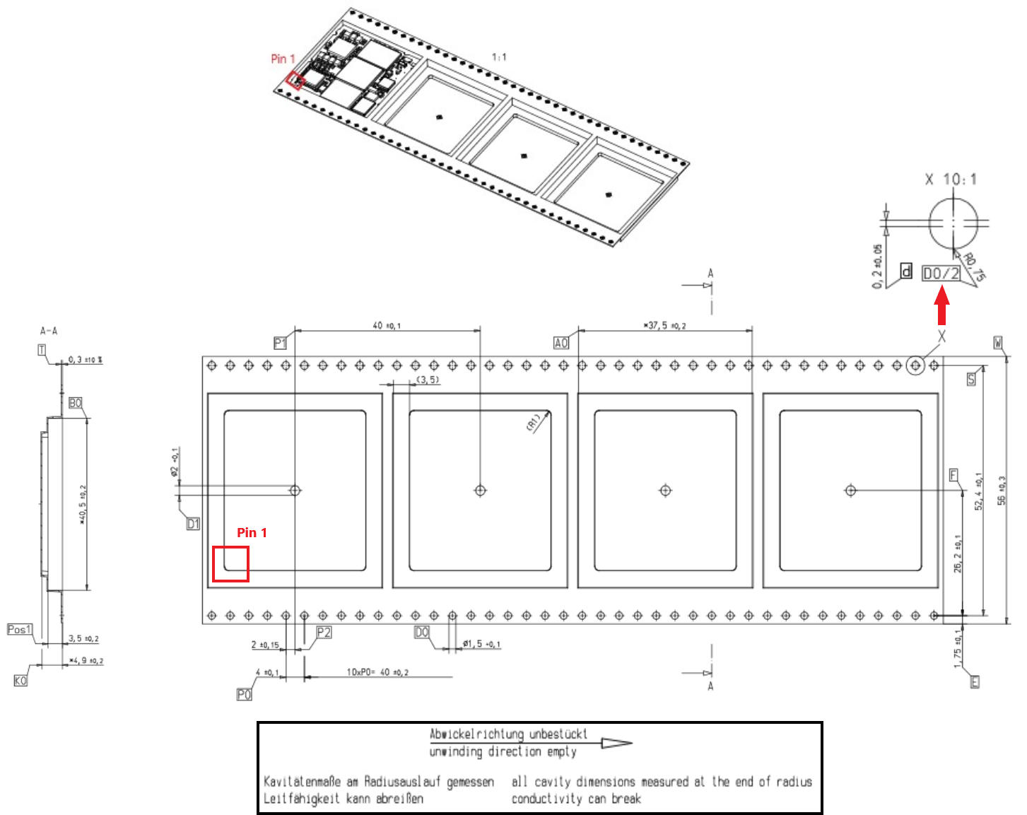
i.MX 8M Mini Reel Technical Information
Production Settings
Moisture Sensitivity, Shelf Life, and Storage
The modules are rated MSL 3, so it is required that they are stored adequately before soldering (see IPC/JEDEC J-STD-033C). PHYTEC recommends storing the modules shrink-wrapped in the original packing. If the packaging is opened, store them in humidity reduced storage (rel. humidity < 10%, T < 30°C / 86°F). The shelf life for sealed packaging is 12 months at < 40°C and < 90 % rel. humidity.
Paste Printing
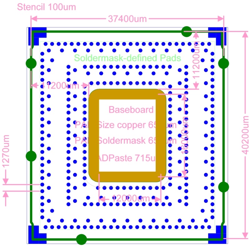
Stencil
- Stencil thickness: 100µm / 4mil
- Stencil alignment: 25% off the smallest pad
- For better durability for mechanical vibrations and shock, the golden edges of the module can be soldered. We did mechanical stress tests without soldered edges and no problems occurred (Shock-Test: 40g, sinusoidal vibrations: 8g at 10 - 150Hz; random noise vibrations: 4g at 10 - 500 Hz). W also did temperature shock tests (750 cycles from -40°C to 125°C) → no problems occurred.
Solder Paste
The following solder paste type has been approved for mounting the module onto a carrier:
- SAC305 (Lead-free: Alpha OM-340 Type 4 or equivalent)
Placement
Dimensions of the Module
The link “phyCORE-i.MX 8M Mini” within the category "Dimensioned Drawing" on the phyCORE‑i.MX 8M Mini download page (https://www.phytec.de/produkt/system-on-modules/phycore-imx-8m-mini-nano-phyboard-polis-download/) leads to the layout data. It is available in different file formats. Use of this data allows integrating the phyCORE-i.MX 8M Mini SOM as a single component into your design.
Coplanarity
The coplanarity measured on the i.MX 8M Mini is<0.003" bow and twist (98% confidence interval). It is important that the carrier board is also coplanar. If the carrier board is thinner then the i.MX 8M Mini, it is recommended that the assembly be supported during the reflow process, i.e. a reflow fixture should be used to minimize the potential bow of the carrier card.
SMT Pick and Place
- Placement Nozzle: Largest nozzle that is available on the machine
- Nozzle Pick Surface: Center of Shield on i.MX 8M Mini SOM
- Placement Speed: Slowest speed for the machine
- Placement alignment: 10% of pad diameter (compensating for module weight and supporting alignment). The module should be placed last as part of the assembly/mounting process to eliminate unexpected shifting.
- Place the SOM at last on the carrier board
SMT Process Parameter Reference
| Process | SMT Process | Specification Recommendations |
|---|---|---|
Screen Print | Solder Paste | Leaded: Indium NC-SMQ92J Lead-free: Alpha OM-340 |
| Stencil Thickness | 0.15 mm / 5 mil | |
| Stencil Diameter | 1.47 mm / 58 mil | |
| Paster Alignment | 25% off the pad (offset <0.25 diameter) | |
PnP | Placement Nozzle | 0>15 mm vacuum |
| Nozzle Pick Surface | PnP cap center | |
| Speed | Slowest speed for the machine | |
| Placement Sequence | Place the SOM last | |
| Placement Alignment | 50% off the pad (offset <.5 diameter) | |
| Reflow | Belt Speed | 0.6-1.1 m/sec |
| Refer to SMT Profile below | ||
Soldering
Our soldering profiles for the vapor phase soldering is based on J-STD-020E (see below). The liquidus time amounts between 60 s and 90 s, and we recommend a maximum of three soldering processes. The peak body temperature of the populated parts is 260°C.
Classification Profile (J-STD-020E1, Table 5-2, Page 8):
| Profile Feature | Pb-Free Assembly |
|---|---|
| Preheat/Soak: Temperature Min (Tsmin) Temperature Max (Tsmax) Time (ts) from (Tsmin to Tsmax) | 150°C 200°C 60-120 seconds |
| Ramp-up Rate (TL to Tp) | 3°C / second max. |
| Liquidus temperature (TL) Time (tL) maintained above TL | 217°C 60-150 seconds |
| Peak Package Body Temperature | For users: Tp must not exceed the classification temperature in Table 4-2. For suppliers: Tp must equal or exceed the classification temperature in Table 4-2. |
| Time (Tp)* within 5°C of the specified classification temperature (Tc), see Figure 5-1. | 30* seconds |
| Ramp-down Rate (Tp to TL) | 6°C / second max. |
| Time 25°C to peak temperature | 8 minutes max |
| *Tolerance for peak profile temperature (Tp) is defined as a supplier minimum and a user maximum. | |
Note 1: All temperatures refer to the center of the package, measured on the package body surface that is facing up during assembly reflow (e.g. live-bug). If parts are reflowed in other than the normal live bug assembly reflow orientation (i.e., dead-bug), Tp must be within±2°C of the livebug Tp and still meet the Tc requirements. Otherwise, the profile must be adjusted to achieve the latter. To accurately measure actual peak package body temperatures, refer to JEP140 for recommended thermocouple use.
Note2: Reflow profiles in this document are for classification / preconditioning and are not meant to specify board assembly profiles. Actual board assembly profiles should be developed based on specific process needs and board designs and should not exceed the parameters in this table. For example, if Tc is 260 °C and time Tp is 30 seconds, this means the following for the supplier and the user:
- For a supplier: The peak temperature must be at least 260 °C. The time above 255 °C must be at least 30 seconds.
- For a user: The peak temperature must not exceed 260 °C. The time above 255 °C must not exceed 30 seconds.
Note 3: All components in the test load must meet the classification profile requirements.
Note 4: SMD packages classified to a given moisture sensitivity level by using Procedures or Criteria defined within any previous version of J-STD-020, JESD22-A112 (rescinded), IPC-SM-786 (rescinded) do not need to be reclassified to the current revision unless a change in classification level or a higher peak classification temperature is desired.
")
Classification Profile (J-STD-020E1, Figure 5-1, Page 8)
1: Revision December 2014
Revision History
Version | Changes | Date | Author |
LAN-095e.A0 | First edition | 12.03.2020 | M. Franck |