Total amount:
plus VAT.
Camera Module Guide - phyCAM-P/phyCAM-S VM-008 Analog Video Digitizer (L-869e.A0)
Table of Contents
Copyrighted products are not explicitly indicated in this manual. The absence of the trademark (TM or ®) and copyright (©) symbols does not imply that a product is not protected. Additionally, registered patents and trademarks are similarly not expressly indicated in this manual.
The information in this document has been carefully checked and is considered to be entirely reliable. However, PHYTEC Messtechnik GmbH assumes no responsibility for any inaccuracies. PHYTEC Messtechnik GmbH neither gives any guarantee nor accepts any liability whatsoever for consequential damages resulting from the use of this manual or its associated product. PHYTEC Messtechnik GmbH reserves the right to alter the information contained herein without prior notification and accepts no responsibility for any damages that might result.
Additionally, PHYTEC Messtechnik GmbH offers no guarantee nor accepts any liability for damages arising from the improper usage or improper installation of the hardware or software. PHYTEC Messtechnik GmbH further reserves the right to alter the layout and/or design of the hardware without prior notification and accepts no liability for doing so.
@ Copyright 2021 PHYTEC Messtechnik GmbH, D-55129 Mainz.
Rights - including those of translation, reprint, broadcast, photomechanical or similar reproduction and storage or processing in computer systems, in whole or in part - are reserved. No reproduction may occur without the express written consent from PHYTEC Messtechnik GmbH.
| EUROPE | NORTH AMERICA | FRANCE | INDIA | CHINA |
Address: | PHYTEC Messtechnik GmbH | PHYTEC America LLC | PHYTEC France | PHYTEC Embedded Pvt. Ltd | PHYTEC Information Technology (Shenzhen) Co. Ltd. |
Ordering Information: | +49 6131 9221-32 | +1 800 278-9913 | +33 2 43 29 22 33 | +91-80-4086 7046/48 sales@phytec.in | +86-755-3395-5875 sales@phytec.cn |
Technical Support: | +49 6131 9221-31 | +1 206 780-9047 | +91-80-4086 7047 support@phytec.in | support@phytec.cn | |
Fax: | +49 6131 9221-33 | +1 206 780-9135 | +33 2 43 29 22 34 | +86-755-3395-5999 | |
Web Site: | http://phytec.in | http://www.phytec.cn |
phyCAM-P VM-008 Analog Video Digitizer
Notes
This manual describes the VM-008 video converter which features both the phyCAM-P and phyCAM-S interface. It can therefore be used in conjunction with controller modules that have either a parallel or an LVDS camera interface.
Default settings in this manual are identified using bold, blue type.
Technical Details
Specifications
- Wide-VGA
- monochrome, color
- 4 inputs for analog video sources
- Various input configurations:
- 4 x CVBS (Composite)
- 3 x CVBS (Composite) and 1 x S-Video
- PAL and NTSC video standard
- Video processor: Brightness, hue, saturation, contrast, and sharpness programmable with software
- Integrated scaler
- phyCAM-S – serial interface connector
- phyCAM-P – parallel interface connector
- Frame rate 25 fps (PAL) / 30 fps (NTSC)
- Status LEDs on all inputs, controllable by application software via I2C interface
- Integrated 4 Kbit EEPROM for application-specific data
(read/write access via I2C interface) - Optional power supply rail for integrated power supply to the cameras.
")
VM-008 Analog Video Digitizer (PCB revision: PL1353.1)
Parameters
| Function | VM-008[1] |
|---|---|
| Video Converter | |
Resolution | (W)VGA |
| 720 x 576 (PAL) |
Sensor Size | n/a |
Pixel Size | n/a |
Color / Monochrome | color and monochrome |
Technology | n/a |
Digitizer | Techwell 9910 |
Scan-System | interlaced |
Shutter-Type | n/a |
Frame rate (fps) | 25 fps (PAL) |
Composite Inputs | 3 (+1) |
S-Video Inputs | 1 |
| Parameter EEPROM 4kBit |
Status LED 4x red, 4x green | |
| Electrical Interface | |
Video Output Type | digital |
Interface | phyCAM-P and phyCAM-S |
Data Format | 8-Bit parallel / 8-Bit serial |
Interface-Mode | YCrCb 4:2:2 |
Dataline-Shifting | - |
Camera Config. Bus | I²C |
Supply Voltage | 3.3V |
Power Consumption | 315 mW (digitizing) |
Pwr. Consumpt. Standby | 106 mW (power-down mode) |
| Mechanical Parameters | |
Dimensions (mm) | 100 x 34 |
Mounting | 4 x M2.5 |
Color (housing) | - |
Weight (standard variant) | 70 g |
Operating Temperature | -25...70°C |
| Connectors | |
| 3 x BNC, 1 x Mini-DIN 4 |
4 x BNC (composite) | |
4 x Mini-DIN 6 (Multifunction) | |
Data and Power | FFC 33-pin (phyCAM-P) |
Hirose DF13A 8-pin (phyCAM-S) | |
| Ext. Power Input for cameras | JST B2B-ZR-SM3 (2-pin) |
VM-008 Parameters
| 1. | n/a: not applicable. All parameters are subject to changes. |
Electrical Specifications
| Symbol | Min. | Typ. | Max. | Unit |
|---|---|---|---|---|---|
Operating Voltage | VCAM | 3.15 | 3.3 | 3.6 | V |
Operating Current | ICAM | - | 95 | 120 | mA |
Digital Input high voltage | VIH | 2.0 | - | VCAM | V |
Digital Input low voltage | VIL | - | - | 0,8 | V |
Output high voltage | VOH | 2.4 | - | VCAM | V |
Output low voltage | VOL | - | 0.2 | 0,4 | V |
Voltage Set Resistor | R31 | - | 0 | 2 | W |
Video Input Amplitude | VVIDEO_IN | 0.5 | 1.00 | 1.40 | V |
Video Input Impedance | - | 75 | W | ||
Camera Supply Voltage | VAUX | - | - | 14 | V |
Camera Supply Current | VAUX (TOTAL) | - | - | 1000 | mA |
Operating Temperature | TOP | -20 | - | 85 | °C |
Storage Temperature | TSTG | -20 | - | 85 | °C |
| Symbol | Min. | Typ. | Max. | Unit |
|---|---|---|---|---|---|
PCLK | fPCLK | 24 | 27 | 30 | MHz |
PCLK Duty Cycle | - | - | - | 55 | % |
PCLK to data valid | tPD | - | 5 | - | ns |
I²C Clock Frequency | fI2C | - | - | 400 | kHz |
| Symbol | Min. | Typ. | Max. | Unit |
|---|---|---|---|---|---|
LVDS Serializer | |||||
Output differential voltage | IVODI | 200 | 270 | - | mV |
VOD change between complementary out states | IDVODI | - | - | 35 | mV |
Output offset voltage | VOS | 0.78 | 1.1 | 1.3 | mV |
VOS change between complementary out states | DVOS | - | - | 35 | mV |
Output current when short to GND | IOS | - | ±30 | ±40 | mA |
Output current in Tri-State | IOZ | - | ±1 | ±10 | µA |
LVDS-Receiver[2] | |||||
Shunt Resistance | RSHUNT | - | 100 | - | W |
| 2. | The board does not have LVDS clock input, shunt for compatibility reasons. |
Data Formats
Monochrome:
- Y8 (processed): 8-bit greyscale
Color:
- YCrCb 4:2:2 (ITU-R 601 / ITU-R 656)
Note
Color mode is automatically switched off and Y8 data format is output for low color amplitude signals, black and white video or very noisy signals, color.
Functional Overview, Block Diagram

VM-008 Block Diagram
The Analog Video Digitizer (AVD) module features 4 inputs for analog video sources. Video inputs can be configured in various ways. It can connect to up to four composite (CVBS) sources or three composite sources and one S-video source at input 3. According to the application requirements, the AVD module can be shipped with various input connectors.
Video signals feed to an internal analog source selector (multiplexer). The digitizer for composite signals is connected to the output of the source selector. The AVD module is capable of digitizing one source at a time. Channel selection is done with software. Channel 3 features either composite or S-video input. The luma component is fed by the source selector into the composite ADC, which digitizes the Y component in this configuration. The chroma component is digitized by a separate A/D converter.
Additional signal processing is carried out, fully digital, by the video processing unit. This includes sync signal detection, Y/C separation, color demodulation, image correction, scaling / cropping, and signal output formatting. The following parameters can be programmed, among others:
- Gain control (optional: AGC)
- Brightness, contrast, saturation, hue (NTSC only), sharpness
- Scaling and cropping (arbitrary downscaling ratios)
- Color or monochrome format
Configuration registers are accessed via the I²C interface.
Digitized image data is available, as a parallel data stream, at the phyCAM-P interface and a serial LVDS data stream at the phyCAM-S interface. Image data consists of 8-bits pixel data, HSYNC, VSYNC, and pixel clock. The data format is YCrCb 4:2:2 (compatible with ITU-R 601 or ITU-R 656). Only one data interface should be used at one time.
The AVD module offers the following additional features:
- Internal Oscillator:The ADV module has an internal oscillator. It is not necessary to provide external master clocks (MCLK).
- LEDs:
Two LEDs (red / green) are located next to each video input connector. The LEDs can be controlled by the application software via the I²C interface and be used for status information, such as green = video signal present, red = channel selected for digitizing. Plastic light guides are available, which makes the LEDs visible at the front panel of a device.An additional LED visualizes the status signal MPOUT of the video processor. Various status information can be assigned to this signal by software. The MPOUT signal is also available at the phyCAM-P – connector.
- I²C-EEPROM:
Application data, such as parameters, can be stored in a serial EEPROM. Read and write accesses are done by the I²C-interface. - Power Supply:
As an option, the power supply of cameras connected to the module can be fed through the input connectors. This requires that the AVD module be populated with a 6-pin Mini-DIN “multifunction” connector. Two pins of these connectors are reserved for an external power supply, which is connected to the module by a 2-pin connector.
Video Inputs
All video inputs have an impedance of 75W. The video inputs can be populated with various connectors.
Configuration | Input 0 | Input 1 | Input 2 | Input 3 |
|---|---|---|---|---|
Configuration 1 | Composite | Composite | Composite | Composite |
BNC | BNC | BNC | BNC | |
Configuration 2 | Composite | Composite | Composite | S-Video |
BNC | BNC | BNC | Mini-DIN 4 | |
Configuration 2 | Composite + Pwr | Composite + Pwr | Composite + Pwr | Composite + Pwr |
Mini-DIN 6 | Mini-DIN 6 | Mini-DIN 6 | Mini-DIN 6 | |
Configuration 2 | Composite + Pwr | Composite + Pwr | Composite + Pwr | S-Video + Pwr |
Mini-DIN 6 | Mini-DIN 6 | Mini-DIN 6 | Mini-DIN 6 |
Composite = CBVS; Pwr = Power supply for camera / external video source
VM-008 Video Input Configurations
The standard variant of the AVD module is equipped with connector Configuration 2. Please inquire with the PHYTEC sales team for other configurations.
Input 3 can operate either in composite or S-video mode. Mode selection is done by software. For S-video, the AVD module must be populated with a 4-pin or 6-pin Mini-DIN connector.
Refer to Section 1.7 for the location of the video connectors.

BNC-connector
| VM-008 - Composite Video Input (BNC Connector) | |||
|---|---|---|---|
Pin | Signal | Dir | Function |
1 | Composite Video In | IN | Composite (CVBS) Video Input |
2 | GND | - | Signal Ground |

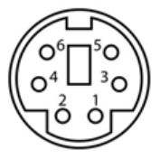
Mini-DIN – connector 4-pin
VM-008 - S-Video Input[3](Mini-DIN Connector) | |||
|---|---|---|---|
Pin | Signal | Dir | Function |
| 1 | GND | - | Signal Ground |
| 2 | GND | - | Signal Ground |
| 3 | S_LUMA | IN | S-Video luma signal (Y) or Composite |
| 4 | S_CHROMA | IN | S-Video chroma signal (C) (channel 3 only) |
| 3. | View on the socket (equivalent plug solder side) |
Mini-DIN – connector 6-pin
| VM-008 - Multifunction-Input (Mini-DIN Connector) | |||
|---|---|---|---|
Pin | Signal | Dir | Function |
| 1 | GND | - | Power Ground |
| 2 | V_CAM_EXT | OUT | Power Out - power supply for camera |
| 3 | GND | - | Signal Ground |
| 4 | GND | - | Signal Ground |
| 5 | S_LUMA | IN | S-Video luma signal (Y) or Composite |
| 6 | S_CHROMA | IN | S-Video chroma signal (C) (channel 3 only) |
Note
The S-video input is available on channel 3 only. However, the S_LUMA – input can be used as a composite input at all channels.
VM-008 phyCAM Interfaces
The AVD module features both a phyCAM-P and a phyCAM-S interface:
- the phyCAM-P interfaces via the connector at X300, located on the bottom side of the AVD module PCB
- the phyCAM-S interfaces via the connector at X305, located on the top side of the AVD module PCB
Notes
- Only one interface can be used at a time.
- CAM_MCLK signal of the phyCAM-P interface is not used by the AVD module. Pin 29 of the connector X300 is not connected.
- The master clock channel of the phyCAM-S – interface is not used by the ADV module. The signal pair LVDS_CLOCK_P and LVDS_CLOCK_N is connected to a 100 W shunt for compatibility reasons. Feeding a clock signal to the AVD module is not necessary.
Image data is transmitted in 8-bit format. Two bytes of data are transmitted for one pixel. The first carries color information, the second transmits brightness.

VM-008 Data Format
Transmission starts with the blue color byte (Cb0), followed by the first brightness byte Y0. A sequence of four bytes contains the color information of one pixel and the brightness information of two pixels (YCrCb 4:2:2 format).
Please note that the video processor has to be set to 8-bit mode. In this mode, the lower data lines VD[7:0] of the video processor are not used. The upper data lines VD[15:8] are connected to the CAM_DD[7:0] output data lines
For more information about the video processor, please refer to the Techwell TW9910 Datasheet.
I2C Addresses
Device | I²C-Address | Jumper Configuration |
|---|---|---|
NTSC/PAL-Converter (TW9910) | 0x8A | J300: 1-2 |
0x88 | J300: 2-3 | |
LED Control (PCA9538) | 0xE0 | J302: 2-3; J303: 2-3 |
0xE2 | J302: 2-3; J303: 1-2 | |
0xE4 | J302 :1-2; J303 :2-3 | |
0xE6 | J302 :1-2; J303 :1-2 | |
EEPROM Bank0 (M24C04) | 0xA4 | J304: 1-2; J305: 2-3 |
EEPROM Bank1 (M24C04) | 0xA6 |
VM-008 I2C Addresses
I²C addresses are shown in hexadecimal, 8-bit notation. Please note that Linux possibly uses 7-bit notation. If developing with 7-bit Linux notation, shift the address value one bit to the right. The table shows the write address (bit 0 = 0). To read from the device, add one to the address (bit 1 = 1).
Note
The I²C address of the user EEPROM can be configured by the jumpers J304 and J305. This is helpful in case of address conflicts with other devices on the bus. See the table below for details.
|
| Jumper Configuration | |
J304 | J305 | ||
EEPROM Bank0 (M24C04) | 0xA4 |
|
|
EEPROM Bank1 (M24C04) | 0xA6 | ||
EEPROM Bank0 (M24C04) | 0xA0 |
|
|
EEPROM Bank1 (M24C04) | 0xA2 | ||
EEPROM Bank0 (M24C04) | 0xA8 |
|
|
EEPROM Bank1 (M24C04) | 0xAA | ||
EEPROM Bank0 (M24C04) | 0xAC |
|
|
EEPROM Bank1 (M24C04) | 0xAE | ||
VM-008 EEPROM I2C Addresses
Feature Pins (phyCAM-P only)
Signal | Pin[4] | Function | I/O | Configuration |
|---|---|---|---|---|
CAM_CTRL1 | 7 | Multi-Purpose Out | O | R314=0R: MPOUT-Signal |
CAM_CTRL2 | 30 | not connected | - | open |
CAM_RST | 3 | /Converter Reset | I | R322=0R: Reset via CAM_RST |
| 4. | Pin numbers relate to X300. |
VM-008 Feature Pins
Notes
Configuration: Internal Configuration of the camera module to activate/use this feature.
NOMT = not mounted
In order to best meet technical requirements and cost objectives, custom configurations are available for high-volume deliveries of phyCAM modules. Please consult PHYTEC for additional information.
Mechanical Dimensions / Jumper Map
")
VM-008 Jumper Map (PCB revision: PL1353.1)

Solder pads colors: blue= top side / red= bottom side
VM-008 Mechanical Dimensions
Special Features
Power LED
A green LED (D200) indicates an active power supply for the AVD module. The LED is labeled PWR on the PCB.
Multi-Purpose Output
The multi-purpose output (MPOUT) of the video processor signals various status information. In standard configuration, the LED labeled MPOUT indicates the selected status information. MPOUT can also be fed to the CAM_CTRL1 pin of the phyCAM-P interface by mounting R314 with a 0 W resistor.
Possible MPOUT signal configurations:
Signal | Description |
|---|---|
Video Loss | 1 = no video signal present on the selected input. |
H-Lock | 1 = H-Sync PLL is locked. |
S-Lock | 1 = Sub-Carrier PLL is locked. |
V-Lock | 1 = V-Sync PLL is locked. |
MONO | 1 = no color burst signal detected. |
DET50 | 1 = 50 Hz – source detected. |
FIELD | 1 = even field is being decoded. |
RTCO | real time control |
0 | (if RTSEL is set to 1111) |
VM-008 Status Information on MPOUT (CAM_CTRL1)
The status LED MPOUT (D306) illuminates yellow if the signal is at an active state (1).
Configuration of status information indicated by MPOUT can be set in register 0x19 (VBICNTL) of the video processor. Note that the highest bit of RTSEL is located in register 0x17.
Note
Status information can also be queried by software via the I²C- interface (register 0x01 - Chip Status Register 1) of the video processor.
Status LEDs
A green and a red LED are placed next to each of the four video inputs. The LEDs are controlled by a GPIO port device via the I2C-interface. This allows the application software to display various status information, such as if a video signal is present at a certain input. The LEDs are located in a manner that allows the optional use of plastic light guides so that the LEDs are visible at the front panel of the AVD module. For that, light guides manufactured by Mentor GmbH are recommended, as described below.
The LEDs are controlled by the I²C device “LED Control” (see I2C Addresses). To activate the LED function, all bits of the data direction register must first be cleared. The LEDs can subsequently be switched on / off by programming the bits of the output register.
Note
A LED is switched on by clearing the corresponding bit of the control register:
Bit state | LED state |
|---|---|
0 | LED on |
1 | LED off (default) |
VM-008 LED State
| LED-Control – Output Register | ||||||||
|---|---|---|---|---|---|---|---|---|
Device0xE0 [5]– Register 0x01 | ||||||||
Bit | D7 | D6 | D5 | D4 | D3 | D2 | D1 | D0 |
Function | LED CH2 | LED CH2 | LED CH2 | LED CH2 | LED CH1 | LED CH1 | LED CH0 | LED CH0 |
VM-008 LED-Control - Output Register
| 5. | default-address. See I2C Addresses |
| LED-Control – Data-Direction Register | ||||||||
|---|---|---|---|---|---|---|---|---|
Device 0xE0[5] – Register 0x03 | ||||||||
| Bit | D7 | D6 | D5 | D4 | D3 | D2 | D1 | D0 |
| Function | 0 | 0 | 0 | 0 | 0 | 0 | 0 | 0 |
VM-008 LED-Control – Data-Direction Register
| 5. | default-address. See I2C Addresses |
Please note that the data direction register defaults to 0xFF. Before using the LED function, the data direction register has to be programmed to 0x00.
The datasheet of PCA9538 provides more information about programming this device.
Plastic light guides can be used to visualize the LEDs at the front panel of the AVD module, next to the video input connectors. PHYTEC recommends the following spherical/planar and countersink light guides from Mentor GmbH, Erkrath, Germany:
www.mentor-bauelemente.de/en/
The positions of the LEDs are optimized for such light guides, which are easily mounted by press-insertion into the panel:
- Spherical / Planar Version

Light Guides Example 1 (drawing: Mentor GmbH)
A | B | C | D | Type | Mentor – Part No. |
|---|---|---|---|---|---|
5.7 | 7.2 | 2.8 | 3.2 | spherical (Example 1- left) | 1282.3000 |
5.7 | 7.2 | 2.8 | 3.2 | planar (Example 1 - right) | 1282.4000 |
2. Countersink Version

Light Guides Example 2 (drawing: Mentor GmbH)
A | B | C | D | Type | Mentor – Part No. |
|---|---|---|---|---|---|
6.2 | 6.6 | 2.8 | 3.2 | countersink (Example 2) | 1282.1200 |
EEPROM
The AVD module features an EEPROM that can store 4 Kb of application-specific data. This memory can be used to store configuration data, serial numbers, and other applicable uses.
The EEPROM is accessed via the I²C interface. The 4 Kb address range is divided into two banks. See I2C Addresses for the I²C device addresses of the two banks. Please note that other EEPROM devices might populate the Carrier Board or target hardware application board to which the AVD module is connected. If an address conflict occurs with other I²C devices on the same bus, the settings of the configuration jumpers J304 / J305 must be changed.
For more information about programming the EEPROM please see the M24C04 Datasheet.
Power Supply for Video Devices
This option enables a single wire connection for video sources that features both video signal and power supply for the video source. To use this option, the AVD module must be populated with a 6-pin Mini-DIN connector. Power supply for the video sources is not generated onboard the AVD module. A power source is connected to X306 of the AVD, which provides a supply voltage of up to 14 V DC for external video sources. Maximum input current is limited to 1A (all devices; current into X306).
The power source for the video devices is connected to X306:
Pin | Dir | Function |
|---|---|---|
1 | - | GND (Ground) |
2 | IN | Input Camera Supply Voltage (positive w/ respect to GND) |
VM-008 X306 Pinout
Connector type: JST B2B-ZR-SM3
Matching housing: JST ZHR-2
The external power supply is protected against reverse polarity by an internal diode and is buffered by a 10µF capacitor. A miniature fuse (F300) protects the external video source supply against over current. In standard configuration, the AVD module is shipped with a 1A fuse installed at F300. Alternatively, fuses with lower ratings can be installed.
The positive pin of the power source must be connected to pin 2 of X306. Pin 1 of the connector at X306 is internally connected to the signal ground of the video digitizer (GND). No potential difference may occur between the negative pin of the external power source for connected video devices and the GND potential of the video decoder.
Mounting Holes
If required, the mounting holes X200, X201, X202, X203 can be connected via capacitors or resistors to the GND plane of the AVD module. This might be useful to improve the EMI behavior of the system.
SMT components with 0805 footprint can be mounted at CB208, CB209, CB210, and CB211.
SBC Kits
Single Board Computer (SBC) kits are available for various microprocessor platforms and operating systems to test camera modules as well as application development. PHYTEC is continuously expanding the platforms supported in these kits. Please refer to the PHYTEC website for the latest information on available kits. Our sales and support team is ready to assist in the selection of appropriate kits and image processing hardware.
Revision History
Date | Version # | Changes in this manual |
|---|---|---|
01.03.2021 | L-869e.A0 | New Manual |
Copyrighted products are not explicitly indicated in this manual. The absence of the trademark (TM or ®) and copyright (©) symbols does not imply that a product is not protected. Additionally, registered patents and trademarks are similarly not expressly indicated in this manual.
The information in this document has been carefully checked and is considered to be entirely reliable. However, PHYTEC Messtechnik GmbH assumes no responsibility for any inaccuracies. PHYTEC Messtechnik GmbH neither gives any guarantee nor accepts any liability whatsoever for consequential damages resulting from the use of this manual or its associated product. PHYTEC Messtechnik GmbH reserves the right to alter the information contained herein without prior notification and accepts no responsibility for any damages that might result.
Additionally, PHYTEC Messtechnik GmbH offers no guarantee nor accepts any liability for damages arising from the improper usage or improper installation of the hardware or software. PHYTEC Messtechnik GmbH further reserves the right to alter the layout and/or design of the hardware without prior notification and accepts no liability for doing so.
@ Copyright 2021 PHYTEC Messtechnik GmbH, D-55129 Mainz.
Rights - including those of translation, reprint, broadcast, photomechanical or similar reproduction and storage or processing in computer systems, in whole or in part - are reserved. No reproduction may occur without the express written consent from PHYTEC Messtechnik GmbH.
| EUROPE | NORTH AMERICA | FRANCE | INDIA | CHINA |
Address: | PHYTEC Messtechnik GmbH | PHYTEC America LLC | PHYTEC France | PHYTEC Embedded Pvt. Ltd | PHYTEC Information Technology (Shenzhen) Co. Ltd. |
Ordering Information: | +49 6131 9221-32 | +1 800 278-9913 | +33 2 43 29 22 33 | +91-80-4086 7046/48 sales@phytec.in | +86-755-3395-5875 sales@phytec.cn |
Technical Support: | +49 6131 9221-31 | +1 206 780-9047 | +91-80-4086 7047 support@phytec.in | support@phytec.cn | |
Fax: | +49 6131 9221-33 | +1 206 780-9135 | +33 2 43 29 22 34 | +86-755-3395-5999 | |
Web Site: | http://phytec.in | http://www.phytec.cn |
phyCAM-P VM-008 Analog Video Digitizer
Notes
This manual describes the VM-008 video converter which features both the phyCAM-P and phyCAM-S interface. It can therefore be used in conjunction with controller modules that have either a parallel or an LVDS camera interface.
Default settings in this manual are identified using bold, blue type.
Technical Details
Specifications
- Wide-VGA
- monochrome, color
- 4 inputs for analog video sources
- Various input configurations:
- 4 x CVBS (Composite)
- 3 x CVBS (Composite) and 1 x S-Video
- PAL and NTSC video standard
- Video processor: Brightness, hue, saturation, contrast, and sharpness programmable with software
- Integrated scaler
- phyCAM-S – serial interface connector
- phyCAM-P – parallel interface connector
- Frame rate 25 fps (PAL) / 30 fps (NTSC)
- Status LEDs on all inputs, controllable by application software via I2C interface
- Integrated 4 Kbit EEPROM for application-specific data
(read/write access via I2C interface) - Optional power supply rail for integrated power supply to the cameras.
VM-008 Analog Video Digitizer (PCB revision: PL1353.1)
Parameters
| Function | VM-008[1] |
|---|---|
| Video Converter | |
Resolution | (W)VGA |
| 720 x 576 (PAL) |
Sensor Size | n/a |
Pixel Size | n/a |
Color / Monochrome | color and monochrome |
Technology | n/a |
Digitizer | Techwell 9910 |
Scan-System | interlaced |
Shutter-Type | n/a |
Frame rate (fps) | 25 fps (PAL) |
Composite Inputs | 3 (+1) |
S-Video Inputs | 1 |
| Parameter EEPROM 4kBit |
Status LED 4x red, 4x green | |
| Electrical Interface | |
Video Output Type | digital |
Interface | phyCAM-P and phyCAM-S |
Data Format | 8-Bit parallel / 8-Bit serial |
Interface-Mode | YCrCb 4:2:2 |
Dataline-Shifting | - |
Camera Config. Bus | I²C |
Supply Voltage | 3.3V |
Power Consumption | 315 mW (digitizing) |
Pwr. Consumpt. Standby | 106 mW (power-down mode) |
| Mechanical Parameters | |
Dimensions (mm) | 100 x 34 |
Mounting | 4 x M2.5 |
Color (housing) | - |
Weight (standard variant) | 70 g |
Operating Temperature | -25...70°C |
| Connectors | |
| 3 x BNC, 1 x Mini-DIN 4 |
4 x BNC (composite) | |
4 x Mini-DIN 6 (Multifunction) | |
Data and Power | FFC 33-pin (phyCAM-P) |
Hirose DF13A 8-pin (phyCAM-S) | |
| Ext. Power Input for cameras | JST B2B-ZR-SM3 (2-pin) |
VM-008 Parameters
| 1. | n/a: not applicable. All parameters are subject to changes. |
Electrical Specifications
| Symbol | Min. | Typ. | Max. | Unit |
|---|---|---|---|---|---|
Operating Voltage | VCAM | 3.15 | 3.3 | 3.6 | V |
Operating Current | ICAM | - | 95 | 120 | mA |
Digital Input high voltage | VIH | 2.0 | - | VCAM | V |
Digital Input low voltage | VIL | - | - | 0,8 | V |
Output high voltage | VOH | 2.4 | - | VCAM | V |
Output low voltage | VOL | - | 0.2 | 0,4 | V |
Voltage Set Resistor | R31 | - | 0 | 2 | W |
Video Input Amplitude | VVIDEO_IN | 0.5 | 1.00 | 1.40 | V |
Video Input Impedance | - | 75 | W | ||
Camera Supply Voltage | VAUX | - | - | 14 | V |
Camera Supply Current | VAUX (TOTAL) | - | - | 1000 | mA |
Operating Temperature | TOP | -20 | - | 85 | °C |
Storage Temperature | TSTG | -20 | - | 85 | °C |
| Symbol | Min. | Typ. | Max. | Unit |
|---|---|---|---|---|---|
PCLK | fPCLK | 24 | 27 | 30 | MHz |
PCLK Duty Cycle | - | - | - | 55 | % |
PCLK to data valid | tPD | - | 5 | - | ns |
I²C Clock Frequency | fI2C | - | - | 400 | kHz |
| Symbol | Min. | Typ. | Max. | Unit |
|---|---|---|---|---|---|
LVDS Serializer | |||||
Output differential voltage | IVODI | 200 | 270 | - | mV |
VOD change between complementary out states | IDVODI | - | - | 35 | mV |
Output offset voltage | VOS | 0.78 | 1.1 | 1.3 | mV |
VOS change between complementary out states | DVOS | - | - | 35 | mV |
Output current when short to GND | IOS | - | ±30 | ±40 | mA |
Output current in Tri-State | IOZ | - | ±1 | ±10 | µA |
LVDS-Receiver[2] | |||||
Shunt Resistance | RSHUNT | - | 100 | - | W |
| 2. | The board does not have LVDS clock input, shunt for compatibility reasons. |
Data Formats
Monochrome:
- Y8 (processed): 8-bit greyscale
Color:
- YCrCb 4:2:2 (ITU-R 601 / ITU-R 656)
Note
Color mode is automatically switched off and Y8 data format is output for low color amplitude signals, black and white video or very noisy signals, color.
Functional Overview, Block Diagram
VM-008 Block Diagram
The Analog Video Digitizer (AVD) module features 4 inputs for analog video sources. Video inputs can be configured in various ways. It can connect to up to four composite (CVBS) sources or three composite sources and one S-video source at input 3. According to the application requirements, the AVD module can be shipped with various input connectors.
Video signals feed to an internal analog source selector (multiplexer). The digitizer for composite signals is connected to the output of the source selector. The AVD module is capable of digitizing one source at a time. Channel selection is done with software. Channel 3 features either composite or S-video input. The luma component is fed by the source selector into the composite ADC, which digitizes the Y component in this configuration. The chroma component is digitized by a separate A/D converter.
Additional signal processing is carried out, fully digital, by the video processing unit. This includes sync signal detection, Y/C separation, color demodulation, image correction, scaling / cropping, and signal output formatting. The following parameters can be programmed, among others:
- Gain control (optional: AGC)
- Brightness, contrast, saturation, hue (NTSC only), sharpness
- Scaling and cropping (arbitrary downscaling ratios)
- Color or monochrome format
Configuration registers are accessed via the I²C interface.
Digitized image data is available, as a parallel data stream, at the phyCAM-P interface and a serial LVDS data stream at the phyCAM-S interface. Image data consists of 8-bits pixel data, HSYNC, VSYNC, and pixel clock. The data format is YCrCb 4:2:2 (compatible with ITU-R 601 or ITU-R 656). Only one data interface should be used at one time.
The AVD module offers the following additional features:
- Internal Oscillator:The ADV module has an internal oscillator. It is not necessary to provide external master clocks (MCLK).
- LEDs:
Two LEDs (red / green) are located next to each video input connector. The LEDs can be controlled by the application software via the I²C interface and be used for status information, such as green = video signal present, red = channel selected for digitizing. Plastic light guides are available, which makes the LEDs visible at the front panel of a device.An additional LED visualizes the status signal MPOUT of the video processor. Various status information can be assigned to this signal by software. The MPOUT signal is also available at the phyCAM-P – connector.
- I²C-EEPROM:
Application data, such as parameters, can be stored in a serial EEPROM. Read and write accesses are done by the I²C-interface. - Power Supply:
As an option, the power supply of cameras connected to the module can be fed through the input connectors. This requires that the AVD module be populated with a 6-pin Mini-DIN “multifunction” connector. Two pins of these connectors are reserved for an external power supply, which is connected to the module by a 2-pin connector.
Video Inputs
All video inputs have an impedance of 75W. The video inputs can be populated with various connectors.
Configuration | Input 0 | Input 1 | Input 2 | Input 3 |
|---|---|---|---|---|
Configuration 1 | Composite | Composite | Composite | Composite |
BNC | BNC | BNC | BNC | |
Configuration 2 | Composite | Composite | Composite | S-Video |
BNC | BNC | BNC | Mini-DIN 4 | |
Configuration 2 | Composite + Pwr | Composite + Pwr | Composite + Pwr | Composite + Pwr |
Mini-DIN 6 | Mini-DIN 6 | Mini-DIN 6 | Mini-DIN 6 | |
Configuration 2 | Composite + Pwr | Composite + Pwr | Composite + Pwr | S-Video + Pwr |
Mini-DIN 6 | Mini-DIN 6 | Mini-DIN 6 | Mini-DIN 6 |
Composite = CBVS; Pwr = Power supply for camera / external video source
VM-008 Video Input Configurations
The standard variant of the AVD module is equipped with connector Configuration 2. Please inquire with the PHYTEC sales team for other configurations.
Input 3 can operate either in composite or S-video mode. Mode selection is done by software. For S-video, the AVD module must be populated with a 4-pin or 6-pin Mini-DIN connector.
Refer to Section 1.7 for the location of the video connectors.
BNC-connector
| VM-008 - Composite Video Input (BNC Connector) | |||
|---|---|---|---|
Pin | Signal | Dir | Function |
1 | Composite Video In | IN | Composite (CVBS) Video Input |
2 | GND | - | Signal Ground |
Mini-DIN – connector 4-pin
VM-008 - S-Video Input[3](Mini-DIN Connector) | |||
|---|---|---|---|
Pin | Signal | Dir | Function |
| 1 | GND | - | Signal Ground |
| 2 | GND | - | Signal Ground |
| 3 | S_LUMA | IN | S-Video luma signal (Y) or Composite |
| 4 | S_CHROMA | IN | S-Video chroma signal (C) (channel 3 only) |
| 3. | View on the socket (equivalent plug solder side) |
Mini-DIN – connector 6-pin
| VM-008 - Multifunction-Input (Mini-DIN Connector) | |||
|---|---|---|---|
Pin | Signal | Dir | Function |
| 1 | GND | - | Power Ground |
| 2 | V_CAM_EXT | OUT | Power Out - power supply for camera |
| 3 | GND | - | Signal Ground |
| 4 | GND | - | Signal Ground |
| 5 | S_LUMA | IN | S-Video luma signal (Y) or Composite |
| 6 | S_CHROMA | IN | S-Video chroma signal (C) (channel 3 only) |
Note
The S-video input is available on channel 3 only. However, the S_LUMA – input can be used as a composite input at all channels.
VM-008 phyCAM Interfaces
The AVD module features both a phyCAM-P and a phyCAM-S interface:
- the phyCAM-P interfaces via the connector at X300, located on the bottom side of the AVD module PCB
- the phyCAM-S interfaces via the connector at X305, located on the top side of the AVD module PCB
Notes
- Only one interface can be used at a time.
- CAM_MCLK signal of the phyCAM-P interface is not used by the AVD module. Pin 29 of the connector X300 is not connected.
- The master clock channel of the phyCAM-S – interface is not used by the ADV module. The signal pair LVDS_CLOCK_P and LVDS_CLOCK_N is connected to a 100 W shunt for compatibility reasons. Feeding a clock signal to the AVD module is not necessary.
Image data is transmitted in 8-bit format. Two bytes of data are transmitted for one pixel. The first carries color information, the second transmits brightness.
VM-008 Data Format
Transmission starts with the blue color byte (Cb0), followed by the first brightness byte Y0. A sequence of four bytes contains the color information of one pixel and the brightness information of two pixels (YCrCb 4:2:2 format).
Please note that the video processor has to be set to 8-bit mode. In this mode, the lower data lines VD[7:0] of the video processor are not used. The upper data lines VD[15:8] are connected to the CAM_DD[7:0] output data lines
For more information about the video processor, please refer to the Techwell TW9910 Datasheet.
I2C Addresses
Device | I²C-Address | Jumper Configuration |
|---|---|---|
NTSC/PAL-Converter (TW9910) | 0x8A | J300: 1-2 |
0x88 | J300: 2-3 | |
LED Control (PCA9538) | 0xE0 | J302: 2-3; J303: 2-3 |
0xE2 | J302: 2-3; J303: 1-2 | |
0xE4 | J302 :1-2; J303 :2-3 | |
0xE6 | J302 :1-2; J303 :1-2 | |
EEPROM Bank0 (M24C04) | 0xA4 | J304: 1-2; J305: 2-3 |
EEPROM Bank1 (M24C04) | 0xA6 |
VM-008 I2C Addresses
I²C addresses are shown in hexadecimal, 8-bit notation. Please note that Linux possibly uses 7-bit notation. If developing with 7-bit Linux notation, shift the address value one bit to the right. The table shows the write address (bit 0 = 0). To read from the device, add one to the address (bit 1 = 1).
Note
The I²C address of the user EEPROM can be configured by the jumpers J304 and J305. This is helpful in case of address conflicts with other devices on the bus. See the table below for details.
|
| Jumper Configuration | |
J304 | J305 | ||
EEPROM Bank0 (M24C04) | 0xA4 |
|
|
EEPROM Bank1 (M24C04) | 0xA6 | ||
EEPROM Bank0 (M24C04) | 0xA0 |
|
|
EEPROM Bank1 (M24C04) | 0xA2 | ||
EEPROM Bank0 (M24C04) | 0xA8 |
|
|
EEPROM Bank1 (M24C04) | 0xAA | ||
EEPROM Bank0 (M24C04) | 0xAC |
|
|
EEPROM Bank1 (M24C04) | 0xAE | ||
VM-008 EEPROM I2C Addresses
Feature Pins (phyCAM-P only)
Signal | Pin[4] | Function | I/O | Configuration |
|---|---|---|---|---|
CAM_CTRL1 | 7 | Multi-Purpose Out | O | R314=0R: MPOUT-Signal |
CAM_CTRL2 | 30 | not connected | - | open |
CAM_RST | 3 | /Converter Reset | I | R322=0R: Reset via CAM_RST |
| 4. | Pin numbers relate to X300. |
VM-008 Feature Pins
Notes
Configuration: Internal Configuration of the camera module to activate/use this feature.
NOMT = not mounted
In order to best meet technical requirements and cost objectives, custom configurations are available for high-volume deliveries of phyCAM modules. Please consult PHYTEC for additional information.
Mechanical Dimensions / Jumper Map
VM-008 Jumper Map (PCB revision: PL1353.1)
Solder pads colors: blue= top side / red= bottom side
VM-008 Mechanical Dimensions
Special Features
Power LED
A green LED (D200) indicates an active power supply for the AVD module. The LED is labeled PWR on the PCB.
Multi-Purpose Output
The multi-purpose output (MPOUT) of the video processor signals various status information. In standard configuration, the LED labeled MPOUT indicates the selected status information. MPOUT can also be fed to the CAM_CTRL1 pin of the phyCAM-P interface by mounting R314 with a 0 W resistor.
Possible MPOUT signal configurations:
Signal | Description |
|---|---|
Video Loss | 1 = no video signal present on the selected input. |
H-Lock | 1 = H-Sync PLL is locked. |
S-Lock | 1 = Sub-Carrier PLL is locked. |
V-Lock | 1 = V-Sync PLL is locked. |
MONO | 1 = no color burst signal detected. |
DET50 | 1 = 50 Hz – source detected. |
FIELD | 1 = even field is being decoded. |
RTCO | real time control |
0 | (if RTSEL is set to 1111) |
VM-008 Status Information on MPOUT (CAM_CTRL1)
The status LED MPOUT (D306) illuminates yellow if the signal is at an active state (1).
Configuration of status information indicated by MPOUT can be set in register 0x19 (VBICNTL) of the video processor. Note that the highest bit of RTSEL is located in register 0x17.
Note
Status information can also be queried by software via the I²C- interface (register 0x01 - Chip Status Register 1) of the video processor.
Status LEDs
A green and a red LED are placed next to each of the four video inputs. The LEDs are controlled by a GPIO port device via the I2C-interface. This allows the application software to display various status information, such as if a video signal is present at a certain input. The LEDs are located in a manner that allows the optional use of plastic light guides so that the LEDs are visible at the front panel of the AVD module. For that, light guides manufactured by Mentor GmbH are recommended, as described below.
The LEDs are controlled by the I²C device “LED Control” (see I2C Addresses). To activate the LED function, all bits of the data direction register must first be cleared. The LEDs can subsequently be switched on / off by programming the bits of the output register.
Note
A LED is switched on by clearing the corresponding bit of the control register:
Bit state | LED state |
|---|---|
0 | LED on |
1 | LED off (default) |
VM-008 LED State
| LED-Control – Output Register | ||||||||
|---|---|---|---|---|---|---|---|---|
Device0xE0 [5]– Register 0x01 | ||||||||
Bit | D7 | D6 | D5 | D4 | D3 | D2 | D1 | D0 |
Function | LED CH2 | LED CH2 | LED CH2 | LED CH2 | LED CH1 | LED CH1 | LED CH0 | LED CH0 |
VM-008 LED-Control - Output Register
| 5. | default-address. See I2C Addresses |
| LED-Control – Data-Direction Register | ||||||||
|---|---|---|---|---|---|---|---|---|
Device 0xE0[5] – Register 0x03 | ||||||||
| Bit | D7 | D6 | D5 | D4 | D3 | D2 | D1 | D0 |
| Function | 0 | 0 | 0 | 0 | 0 | 0 | 0 | 0 |
VM-008 LED-Control – Data-Direction Register
| 5. | default-address. See I2C Addresses |
Please note that the data direction register defaults to 0xFF. Before using the LED function, the data direction register has to be programmed to 0x00.
The datasheet of PCA9538 provides more information about programming this device.
Plastic light guides can be used to visualize the LEDs at the front panel of the AVD module, next to the video input connectors. PHYTEC recommends the following spherical/planar and countersink light guides from Mentor GmbH, Erkrath, Germany:
www.mentor-bauelemente.de/en/
The positions of the LEDs are optimized for such light guides, which are easily mounted by press-insertion into the panel:
- Spherical / Planar Version
Light Guides Example 1 (drawing: Mentor GmbH)
A | B | C | D | Type | Mentor – Part No. |
|---|---|---|---|---|---|
5.7 | 7.2 | 2.8 | 3.2 | spherical (Example 1- left) | 1282.3000 |
5.7 | 7.2 | 2.8 | 3.2 | planar (Example 1 - right) | 1282.4000 |
2. Countersink Version
Light Guides Example 2 (drawing: Mentor GmbH)
A | B | C | D | Type | Mentor – Part No. |
|---|---|---|---|---|---|
6.2 | 6.6 | 2.8 | 3.2 | countersink (Example 2) | 1282.1200 |
EEPROM
The AVD module features an EEPROM that can store 4 Kb of application-specific data. This memory can be used to store configuration data, serial numbers, and other applicable uses.
The EEPROM is accessed via the I²C interface. The 4 Kb address range is divided into two banks. See I2C Addresses for the I²C device addresses of the two banks. Please note that other EEPROM devices might populate the Carrier Board or target hardware application board to which the AVD module is connected. If an address conflict occurs with other I²C devices on the same bus, the settings of the configuration jumpers J304 / J305 must be changed.
For more information about programming the EEPROM please see the M24C04 Datasheet.
Power Supply for Video Devices
This option enables a single wire connection for video sources that features both video signal and power supply for the video source. To use this option, the AVD module must be populated with a 6-pin Mini-DIN connector. Power supply for the video sources is not generated onboard the AVD module. A power source is connected to X306 of the AVD, which provides a supply voltage of up to 14 V DC for external video sources. Maximum input current is limited to 1A (all devices; current into X306).
The power source for the video devices is connected to X306:
Pin | Dir | Function |
|---|---|---|
1 | - | GND (Ground) |
2 | IN | Input Camera Supply Voltage (positive w/ respect to GND) |
VM-008 X306 Pinout
Connector type: JST B2B-ZR-SM3
Matching housing: JST ZHR-2
The external power supply is protected against reverse polarity by an internal diode and is buffered by a 10µF capacitor. A miniature fuse (F300) protects the external video source supply against over current. In standard configuration, the AVD module is shipped with a 1A fuse installed at F300. Alternatively, fuses with lower ratings can be installed.
The positive pin of the power source must be connected to pin 2 of X306. Pin 1 of the connector at X306 is internally connected to the signal ground of the video digitizer (GND). No potential difference may occur between the negative pin of the external power source for connected video devices and the GND potential of the video decoder.
Mounting Holes
If required, the mounting holes X200, X201, X202, X203 can be connected via capacitors or resistors to the GND plane of the AVD module. This might be useful to improve the EMI behavior of the system.
SMT components with 0805 footprint can be mounted at CB208, CB209, CB210, and CB211.
SBC Kits
Single Board Computer (SBC) kits are available for various microprocessor platforms and operating systems to test camera modules as well as application development. PHYTEC is continuously expanding the platforms supported in these kits. Please refer to the PHYTEC website for the latest information on available kits. Our sales and support team is ready to assist in the selection of appropriate kits and image processing hardware.
Revision History
Date | Version # | Changes in this manual |
|---|---|---|
01.03.2021 | L-869e.A0 | New Manual |