Gesamtbetrag:
zzgl. Mwst.
Soldering Guide - i.MX 8M Plus Fused Tin Grid Array (FTGA) Information (LAN-112e.A0)
Table of Contents
Introduction
This guide provides information on how to solder the various phyCORE-i.MX 8M Plus modules.
Tip
- For good soldering results, we recommend using the parameters in this guide as much as possible. Variations to the parameters may cause issues when soldering a phyCORE module.
- Due to its weight and to reduce the soldering cycles, we recommend populating the SOM onto the assembly side of the carrier board with the SOM's assembly-side facing upwards.
- For technical support or additional information, please contact our technical support team.
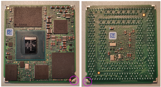
phyCORE-i.MX 8M Plus Module
Delivery Format
The modules are only shipped in reels. For more information, please contact PHYTEC Sales.
All dimensions and tolerances are as per EIA 481 standard.
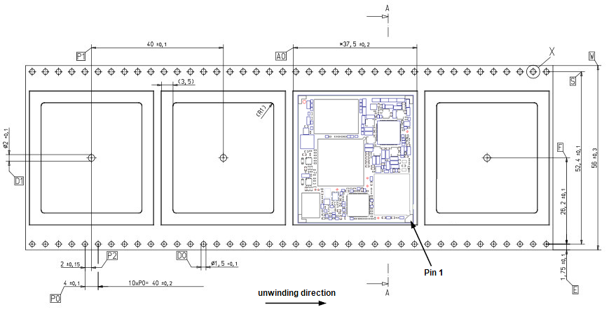
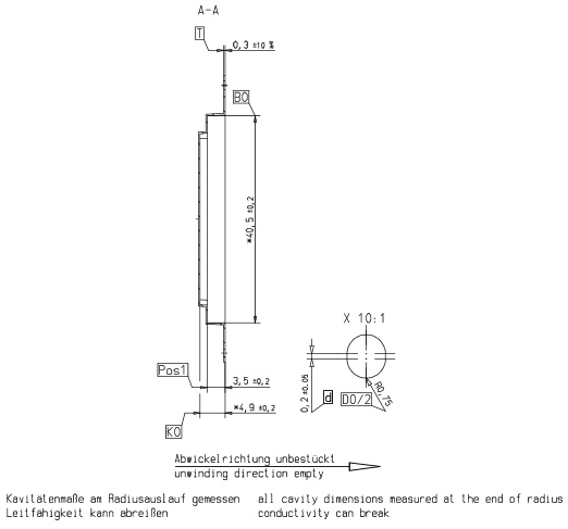
i.MX 8M Plus Reel Technical Information
Production Settings
Moisture Sensitivity, Shelf Life, and Storage
The modules are rated MSL 3, so it is required that they are stored adequately before soldering (see IPC/JEDEC J-STD-033C). PHYTEC recommends storing the modules shrink-wrapped in the original packing. If the packaging is opened, store them in humidity-reduced storage (rel. humidity < 10%, T < 30°C / 86°F). The shelf life for sealed packaging is 12 months at < 40°C and < 90 % rel. humidity.
Paste Printing
Stencil
- Stencil thickness: 100µm / 4mil
- Stencil alignment: 25% off the smallest pad
- Use two 0402 preforms for each soldering edge and expand the paste opening by 100 µm
- The alloy of 0402 preforms should also be SAC305 (identical to the solder paste)
Solder Paste
The following solder paste type has been approved for mounting the module onto a carrier:
- SAC305 (Lead-free: Indium8.9HF 88,5% Type 4 or equivalent)
Placement

Dimensions of the Module
The link “phyCORE-i.MX 8M Plus” is within the category "Dimensioned Drawing" on the phyCORE‑i.MX 8M Plus download page (https://www.phytec.de/produkte/system-on-modules/phycore-imx-8m-plus/#downloads/) leads to the layout data. It is available in different file formats. The use of this data allows for the integration of the phyCORE-i.MX 8M Plus SOM as a single component in your design.
Cut Out
Place a 15 mm x 18 mm cutout for the bottom side components of the SOM.
Coplanarity
The coplanarity measured on the i.MX 8M Plus is<0.003" bow and twist (98% confidence interval). It is important that the carrier board is also coplanar. If the carrier board is thinner than the i.MX 8M Plus, it is recommended that the assembly be supported during the reflow process, i.e. a reflow fixture should be used to minimize the potential bow of the carrier card.
SMT Pick and Place

SMT Pick and Place Dimensions
- Placement Nozzle: Largest nozzle that will fit
- Nozzle Pick Surface: Center of Shield on i.MX 8M Plus CPU
- Placement Speed: Slowest speed for the machine
- Placement alignment: 10% of pad diameter (compensating for module weight and supporting alignment)
- Place the SOM at last part of the carrier board to eliminate unexpected shifting
SMT Process Parameter Reference
| Process | SMT Process | Specification Recommendations |
|---|---|---|
Screen Print | Solder Paste | SAC305: Indium8.9HF 88,5% Type 4 or equivalent |
| Stencil Thickness | 0.1 mm / 4 mil | |
Stencil Pad Diameter Stencil Soldering Edges | 0.72 mm / 28 mil Overprint by 100 µm / 40 mil | |
| Paster Alignment | 25% off the pad (offset <0.25 diameter) | |
PnP | SOM weight | approx. 8g |
| Placement Nozzle | 0>15 mm vacuum | |
| Nozzle Pick Surface | PnP cap center | |
| Speed | Slowest speed for the machine | |
| Placement Sequence | Place the SOM last | |
| Placement Alignment | 50% off the pad (offset <.5 diameter) | |
| Reflow | Belt Speed | 0.6-1.1 m/sec |
| Refer to SMT Profile below | ||
SMT Process Parameter References
Soldering
It is strongly recommended that the module be melted entirely through. This is the case with our in-house processing. This is not harmful to the module and results in the most resilient solder joints. All of the soldered connections that we examined externally were completely melted through again when the DSC module and the baseboard were soldered. All components of the module can be seen as regular SMD components and are to be soldered together with the motherboard according to the JEDEC soldering profile recommendation.
Our soldering profiles for the vapor phase soldering are based on J-STD-020E[1](see below). The liquidus time amounts between 60 s and 90 s, and we recommend a maximum of three soldering processes. The peak body temperature of the populated parts is 260°C.
| Profile Feature | Pb-Free Assembly |
|---|---|
| Preheat/Soak: Temperature Min (Tsmin) Temperature Max (Tsmax) Time (ts) from (Tsmin to Tsmax) | 150°C 200°C 60-120 seconds |
| Ramp-up Rate (TL to Tp) | 3°C / second max. |
| Liquidus temperature (TL) Time (tL) maintained above TL | 217°C 60-150 seconds |
| Peak Package Body Temperature | For users: Tp must not exceed the classification temperature in Table 4-2. For suppliers: Tp must equal or exceed the classification temperature in Table 4-2. |
| Time (Tp)* within 5°C of the specified classification temperature (Tc), see Figure 5-1. | 30* seconds |
| Ramp-down Rate (Tp to TL) | 6°C / second max. |
| Time 25°C to peak temperature | 8 minutes max |
| *Tolerance for peak profile temperature (Tp) is defined as a supplier minimum and a user maximum. | |
Classification Profile (J-STD-020E, Table 5-2, Page 8)
Note 1: All temperatures refer to the center of the package, measured on the package body surface facing up during assembly reflow (e.g. live-bug). If parts are reflowed in other than the normal live bug assembly reflow orientation (i.e., dead bug), Tp must be within±2°C of the live bug Tp and still meet the Tc requirements. Otherwise, the profile must be adjusted to achieve the latter. To accurately measure actual peak package body temperatures, refer to JEP140 for recommended thermocouple use.
Note 2: Reflow profiles in this document are for classification/preconditioning and are not meant to specify board assembly profiles. Actual board assembly profiles should be developed based on specific process needs and board designs and should not exceed the parameters in this table. For example, if Tc is 260 °C and time Tp is 30 seconds, this means the following for the supplier and the user:
- For a supplier: The peak temperature must be at least 260 °C. The time above 255 °C must be at least 30 seconds.
- For a user: The peak temperature must not exceed 260 °C. The time above 255 °C must not exceed 30 seconds.
Note 3: All components in the test load must meet the classification profile requirements.
Note 4: SMD packages classified to a given moisture sensitivity level by using Procedures or Criteria defined within any previous version of J-STD-020, JESD22-A112 (rescinded), IPC-SM-786 (rescinded) do not need to be reclassified to the current revision[1] unless a .change in classification level or a higher peak classification temperature is desired.
")
Classification Profile (J-STD-020E, Figure 5-1, Page 8)
| 1. | Revision December 2014 |
Revision History
Version | Changes | Date |
LAN-112e.A0 | Preliminary Edition | 12.12.2022 |
.