Gesamtbetrag:
zzgl. Mwst.
Hardware Manual - phyCORE-STM32MP15x/phyBOARD-Sargas (1534.1/1517.2) (L-875e.A2)
Table of Contents
Preface
As a member of PHYTEC's phyCORE® product family, the phyCORE‑STM32MP15x is one of a series of PHYTEC System on Modules (SOMs) that can be populated with different controllers and, therefore, offers various functions and configurations. PHYTEC supports a variety of 8/16/32/64 bit controllers in two ways:
(1) As the basis for Rapid Development Kits which serve as a reference and evaluation platform
(2) As insert-ready, fully functional phyCORE® OEM modules, which can be embedded directly into the user’s peripheral hardware design.
Implementation of an OEM-able SOM subassembly as the "core" of your embedded design allows for increased focus on hardware peripherals and firmware without expending resources to "re-invent" microcontroller circuitry. Furthermore, much of the value of the phyCORE® module lies in its layout and test.
Production-ready Board Support Packages (BSPs) and Design Services for our hardware will further reduce development time and risk and allows for increased focus on product expertise. Take advantage of PHYTEC products to shorten time-to-market, reduce development costs, and avoid substantial design issues and risks. With this new innovative full system solution, new ideas can be brought to market in the most timely and cost-efficient manner.
For more information go to:
http://www.phytec.de/de/leistungen/entwicklungsunterstuetzung.html
or
http://www.phytec.eu/europe/oem-integration/evaluation-start-up.html
Ordering Information
The part numbering of the phyCORE has the following structure:

Product Specific Information and Technical Support
In order to receive product-specific information on all future changes and updates, we recommend registering at:
http://www.phytec.de/de/support/registrierung.html or http://www.phytec.eu/europe/support/registration.html
For technical support and additional information concerning your product, please visit the support section of our website which provides product-specific information, such as errata sheets, application notes, FAQs, etc.
https://www.phytec.de/produkte/system-on-modules/phycore-stm32mp15x/
or
https://www.phytec.eu/en/produkte/system-on-modules/phycore-stm32mp15x
Declaration of Electro Magnetic Conformity of the PHYTEC phyCORE®‑STM32MP15x 

PHYTEC System on Module (henceforth products) are designed for installation in electrical appliances or as dedicated Evaluation Boards (i.e.: for use as a test and prototype platform for hardware/software development) in laboratory environments.
Warning
PHYTEC products lacking protective enclosures are subject to damage by ESD and, therefore, must be unpacked, handled, or operated in environments in which sufficient precautionary measures have been taken with respect to ESD dangers. It is also necessary that only appropriately trained personnel (such as electricians, technicians, and engineers) handle and/or operate these products. Moreover, PHYTEC products should not be operated without protection circuitry if connections to the product's pin header rows are longer than 3 m.
PHYTEC products fulfill the norms of the European Union’s Directive for Electro Magnetic Conformity only in accordance with the descriptions and rules of usage indicated in this hardware manual (particularly with respect to the pin header row connectors, power connector, and serial interface to a host-PC).
Implementation of PHYTEC products into target devices, as well as user modifications and extensions of PHYTEC products, is subject to renewed establishment of conformity to, and certification of, Electro Magnetic Directives. Users should ensure conformance following any modifications to the products as well as the implementation of the products into target systems.
Product Change Management and Information Regarding Parts Populated on the SOM / Carrier Board
With the purchase of a PHYTEC SOM / Carrier Board, you will, in addition to our HW and SW offerings, receive free obsolescence maintenance service for the hardware we provide. Our PCM (Product Change Management) Team of developers, is continuously processing, all incoming PCNs (Product Change Notifications) from vendors and distributors concerning parts that are used in our products.
Possible impacts on the functionality of our products, due to changes in functionality or obsolesce of a certain part, are constantly being evaluated in order to take the right measures in purchasing or within our hardware/software design.
Our general philosophy here is: We never discontinue a product as long as there is a demand for it.
Therefore, we have established a set of methods to fulfill our philosophy:
Avoiding strategies:
- Avoid changes by evaluating the longevity of parts during the design-in phase.
- Ensure the availability of equivalent second source parts.
- Stay in close contact with part vendors to be aware of roadmap strategies.
Change management in the rare event of an obsolete and non-replaceable part:
- Ensure long-term availability by stocking parts through last-time buy management according to product forecasts.
- Offer long-term frame contracts to customers.
Change management in case of functional changes:
- Avoid impacts on product functionality by choosing equivalent replacement parts.
- Avoid impacts on product functionality by compensating changes through HW redesign or backward-compatible SW maintenance.
- Provide early change notifications concerning functional relevant changes to our products.
Therefore, we refrain from providing detailed part-specific information within this manual, which can be subject to continuous changes, due to part maintenance for our products.
In order to receive reliable, up-to-date, and detailed information concerning parts used for our product, please contact our support team through the contact information given within this manual.
PHYTEC Documentation
PHYTEC will provide a variety of hardware and software documentation for all of our products. This includes any or all of the following:
- QS Guide: A short guide on how to set up and boot a phyCORE board along with brief information on building a BSP, the device tree, and accessing peripherals.
- Hardware Manual: A detailed description of the System on Module and accompanying carrier board.
- Yocto Guide: A comprehensive guide for the Yocto version the phyCORE uses. This guide contains an overview of Yocto; an introduction, installing and customizing the PHYTEC BSP; how to work with programs like Poky and Bitbake; and much more.
- BSP Manual: A manual specific to the BSP version of the phyCORE. Information such as how to build the BSP, booting, updating software, device tree, and accessing peripherals can be found here.
- Development Environment Guide: This guide shows how to work with the pre-programmed programs Eclipse and Qt Creator. It includes instructions for running demo projects for these programs on a phyCORE product. Information on how to set up a Linux host PC is also included.
- Pin Muxing Table: Starting in 2019, all phyCORE SOMs will have an accompanying pin table (in Excel format). This table will show the complete default signal path, from processor to carrier board. The default device tree muxing option will also be included. This gives a developer all the information needed in one location to make muxing changes and design options when developing a specialized carrier board or adapting a PHYTEC phyCORE SOM to an application.
On top of these standard manuals and guides, PHYTEC will also provide Product Change Notifications, Application Notes, and Technical Notes. These will be done on a case-by-case basis. All documentation can be found on the applicable download page of our products.
Conventions, Abbreviations, and Acronyms
This hardware manual describes the PCM-068 System on Module, referred to as phyCORE‑STM32MP15x, and the corresponding single-board computer PCM-939, the phyBOARD-Sargas STM32MP15x. The manual specifies phyCORE‑STM32MP15x and phyBOARD-Sargas's design and function. Precise specifications for the STMicroelectronics® STM32MP15x microcontrollers can be found in the enclosed Microcontroller Data Sheet/User's Manual.
Note
We refrain from providing detailed, part-specific information within this manual (due to part maintenance for our products), which can be subject to continuous changes. Please read the section Product Change Management and Information Regarding Parts Populated on the SOM / Carrier Board within the Preface.
Note
The BSP delivered with the phyCORE®-STM32MP15x usually includes drivers and/or software for controlling all components such as interfaces, memory, etc. Programming close to hardware at the register level is not necessary in most cases. For this reason, this manual contains no detailed description of the controller's registers or information relevant to software development. Please refer to the STM32MP157C Reference Manual, if such information is needed to connect customer-designed applications.
Conventions
The conventions used in this manual are as follows:
- Signals that are preceded by an "n", "/", or “#” character (e.g.: nRD, /RD, or #RD), or that have a dash on top of the signal name are designated as active low signals. That is, their active state is when they are driven low or are driving low.
- A "0" indicates a logic zero or low-level signal, while a "1" represents a logic one or high-level signal.
- The hex numbers given for addresses of I2C devices always represent the 7 MSB of the address byte. The correct value of the LSB which depends on the desired command (read (1), or write (0)) must be added to get the complete address byte. E.g. given address in this manual 0x41 => complete address byte = 0x83 to read from the device and 0x82 to write to the device
- Tables that describe jumper settings show the default position in bold,bluetext.
- Text in blue italic indicates a hyperlink within, or external to the document. Click these links to quickly jump to the applicable URL, part, chapter, table, or figure.
- References made to the phyCORE-Connector always refer to the high-density Samtec connector on the undersides of the phyCORE‑STM32MP15x System on Module.
Types of Signals
Different types of signals are brought out at the phyCORE-Connector. The following table lists the abbreviations used to specify the type of signal.
Signal Type | Description | Abbreviation |
|---|---|---|
Power | Supply voltage input | PWR_I |
Power | Supply voltage output | PWR_O |
Ref-Voltage | Reference voltage output | REF_O |
Input | Digital input | I |
Output | Digital output | O |
IO | Bidirectional input/output | I/O |
OC-Bidir PU | Open collector input/output with pull up | OC-BI |
OC-Output | Open collector output without pull up requires an external pull up | OC |
OD-Output | Open-drain output without pull up requires an external pull up | OD |
5V Input PD | 5 V tolerant input with a pull-down | 5V_PD |
LVDS Input | Differential line pairs 100 Ohm LVDS level input | LVDS_I |
LVDS Output | Differential line pairs 100 Ohm LVDS level output | LVDS_O |
TMDS Output | Differential line pairs 100 Ohm TMDS level output | TMDS_O |
USB IO | Differential line pairs 90 Ohm USB level bidirectional input/output | USB_I/O |
ETHERNET Input | Differential line pairs 100 Ohm Ethernet level input | ETH_I |
ETHERNET Output | Differential line pairs 100 Ohm Ethernet level output | ETH_O |
ETHERNET IO | Differential line pairs 100 Ohm Ethernet level bidirectional input/output | ETH_I/O |
MIPI DSI Output | Differential line pairs 100 Ohm MIPI DSI level output | DSI_O |
Signal Types
Abbreviations and Acronyms
Many acronyms and abbreviations are used throughout this manual. Use this table to navigate unfamiliar terms used in this document.
| Abbreviation | Definition |
|---|---|
BSP | Board Support Package (Software delivered with the Development Kit including an operating system (Windows, or Linux) preinstalled on the module and Development Tools). |
CB | Carrier Board; used in reference to the phyCORE Development Kit Carrier Board. |
DFF | D flip-flop. |
EMB | External memory bus. |
EMI | Electromagnetic Interference. |
GPI | General-purpose input. |
GPIO | General-purpose input and output. |
GPO | General-purpose output. |
IRAM | Internal RAM; the internal static RAM on the STMicroelectronics® STM32MP15x microcontroller. |
J | Solder jumpers; these types of jumpers require solder equipment to remove and place. |
JP | Solderless jumpers; these types of jumpers can be removed and placed by hand with no special tools. |
PCB | Printed circuit board. |
PDI | PHYTEC Display Interface; defined to connect PHYTEC display adapter boards, or custom adapters |
PEB | PHYTEC Extension Board |
PMIC | Power management IC |
PoE | Power over Ethernet |
POR | Power-on reset |
RTC | Real-time clock. |
SMT | Surface mount technology. |
SOM | System on Module; used in reference to the PCM-068 /phyCORE®-STM32MP15x module |
Sx | User button Sx (e.g. S1, S2, etc.) used in reference to the available user buttons, or DIP-Switches on the carrier board. |
Sx_y | Switch y of DIP-Switch Sx; used in reference to the DIP-Switch on the carrier board. |
Abbreviations and Acronyms
phyCORE‑STM32MP15x Introduction
The phyCORE‑STM32MP15x belongs to PHYTEC’s phyCORE System on Module family. The phyCORE SOMs represent the continuous development of the PHYTEC System on Module technology. Like its mini-, micro-, and nano MODUL predecessors, phyCORE boards integrate all core elements of a microcontroller system on a sub-miniature board and are designed in a manner that ensures their easy expansion and embedding in peripheral hardware developments.
Independent research indicates approximately 70 % of all EMI (Electro-Magnetic Interference) problems are caused by insufficient supply voltage grounding of electronic components in high-frequency environments. The phyCORE board design features an increased pin package, which provides for the dedication of approximately 20 % of all connector pinson the phyCORE boards to Ground. This improves EMI and EMC characteristics and makes it easier to design complex applications meeting EMI and EMC guidelines using phyCORE boards, even in high-noise environments.
phyCORE boards achieve their small size through modern SMD technology and multi-layer design. In accordance with the complexity of the module, 0201-packaged SMT components and laser-drilled microvias are used on the boards, providing phyCORE users with access to this cutting-edge miniaturization technology for integration into their own design.
The phyCORE‑STM32MP15x is a sub-miniature (40 mm x 44 mm) insert-ready System on Module populated with the STMicroelectronics® STM32MP15x microcontroller. Its universal design enables its insertion in a wide range of embedded applications. All controller signals and ports extend from the controller to high-density pitch, or surface mount technology (SMT) connectors (all pitch 0.5 mm) aligning two sides of the board, allowing it to be plugged or soldered into any target application like a "big chip".
The descriptions in this manual are based on the STMicroelectronics STM32MP157C. No description of compatible microcontroller derivative functions is included as such functions are not relevant for the basic functioning of the phyCORE‑STM32MP15x. Precise specifications for the controller populating the board can be found in the applicable controller technical reference manual or datasheet.
Note
- Most of the controller pins have multiple multiplexed functions. As most of these pins are connected directly to the phyCORE-Connector, the alternative functions are available by using the STM32MP15x's pin muxing options. However, the following list of features is in regard to the specification of the phyCORE‑STM32MP15x and the functions defined therein. Therefore, theindicatednumberofcertaininterfaces,CSsignals,etc.isperhapssmallerthanavailableonthecontroller. Please refer to the STM32MP157C Reference Manual to learn more about alternative functions. In order to utilize a specific pin's alternative function, the corresponding registers and the device tree must be configured within the appropriate driver of the BSP.
Tip
- STMicroelectronics provides software for pin muxing. For further information about the pin muxing tool, refer to STM32CubeMX.
phyCORE‑STM32MP15x Features
The phyCORE‑STM32MP15x offers the following features:
- Insert-ready, sub-miniature (44 mm x 40 mm) System on Module (SOM) sub-assembly in low EMI design, achieved through advanced SMT technology
Populated with the STMicroelectronics® STM32MP157C[1]microcontroller (TFBGA361 packaging)
- Up to 2 ARM-Cortex-A7 cores (clock frequency up to 800 MHz) + ARM-Cortex-M4 core up to 209 MHz
- Boot from different memory devices (SD card, QSPI NOR-Flash, NAND-Flash, eMMC)
- Controller signals and ports extend to two high-density pitch (0.5 mm) Samtec connectors aligning two sides of the board, enabling the phyCORE‑STM32MP15x to be plugged into any target applications like a "big chip"
- Single supply voltage of +5.0 V with on-board power management
- All controller-required supplies are generated on-board
- Improved interference safety achieved through multi-layer PCB technology and dedicated ground pins
256 MB (up to 1 GB[2]) 32-bit wide DDR3L RAM
- 4 GB (up to 32 GB[2]) onboard eMMC, or 128 MB (up to 1 GB[2]) onboard SLC NAND flash
- 4 MB (up to 16 MB[2])Quad SPI NOR flash (bootable)
- 4 kB (up to 32 kB[2]) I2C EEPROM
- 4x UART interfaces
- 2x High-speed USB 2.0 interfaces (1 x USB host and 1 x USB OTG)
- 1x 10/100/1000 Mbit/s Ethernet interface. Either with Ethernet transceiver on the phyCORE‑STM32MP15x, allowing for direct connection to an existing Ethernet network, or without an onboard transceiver and provision of the RGMII signals at TTL-level (10/100/1000 Mbit/s) at the phyCORE‑Connector instead[1]
- 2x I2C interfaces
- 2x SPI interfaces (NAND/QSPI)
- 1x CAN FD interface
- 1x MIPI DSI interface
- 1x Parallel 18-bit RGB display interface with HDMI-CEC
- 1x 10-bit parallel camera interface
- 1x SAI Audio interface
- 1x MDIO interface
3x Secure Digital I/O MultiMediaCard interfaces (SDMMC) up to 8-bit (SD / eMMC / SDIO)
Several dedicated GPIOs[3]
- Several AD conversion and filter inputs digital (DFSDM)
- 2x 12-bit DAC outputs
- 1x JTAG/Serial-wire debug interface with trace ports and debug trigger I/Os
- I2C Real-Time Clock[1] with a very low-power operation, independent from CPU-supply
- Power Management IC (PMIC)
- Available for different temperature grades (Product Temperature Grades)
Warning
Samtec connectors guarantee optimal connection and proper insertion of the phyCORE‑STM32MP15x. Please make sure that the STM32MP15x module is fully plugged into the mating connectors of the carrier board. Otherwise, individual signals may have bad contact or no contact at all.
| 1. | Please refer to the order options described in the Preface, or contact PHYTEC for more information about |
| 2. | The maximum memory size listed is as of the printing of this manual. |
| 3. | Almost every controller port which connects directly to the phyCORE-Connector may be used |
phyCORE‑STM32MP15x Block Diagram
phyCORE‑STM32MP15x Block Diagram
phyCORE‑STM32MP15x Component Placement
phyCORE‑STM32MP15x Component Placement (Top View)
")
phyCORE‑STM32MP15x Component Placement (Bottom View)
phyCORE‑STM32MP15x Minimum Operating Requirements
Warning
We recommend connecting all available +5 V input pins to the power supply system on a custom carrier board housing the phyCORE‑STM32MP15x and, at minimum, the matching number of GND pins neighboring the +5 V pins. In addition, proper implementation of the phyCORE‑STM32MP15x module into a target application also requires connecting all GND pins. Refer to sectionPower for more information.
Pin Description
Warning
Module connections must not exceed their expressed maximum voltage or current. Maximum signal input values are indicated in the corresponding controller manuals/datasheets. As damage from improper connections varies according to use and application, it is the user's responsibility to take appropriate safety measures to ensure that the module connections are protected from overloading through connected peripherals.
As the imagePinout of the phyCORE-Connector indicates, all controller signals selected extend to surface mount technology (SMT) connectors (0.5 mm). These connectors line two sides of the module (referred to as phyCORE-Connectors). This enables the phyCORE‑STM32MP15x to be plugged into any target application like a "big chip".
The numbered scheme for the phyCORE‑Connector is based on a two-dimensional matrix in which column positions are identified by a letter and row positions by a number. The pin numbering values increase as you move across the board from left to right. The numbered matrix can be aligned with the phyCORE‑STM32MP15x (viewed from above; phyCORE‑Connector pointing down) or with the socket of the corresponding phyCORE carrier board/user target circuitry. The upper left-hand corner of the numbered matrix (pin X1A1) is covered by the corner of the phyCORE‑STM32MP15x. The numbering scheme is always in relation to the PCB as viewed from above, even if all connector contacts extend to the bottom of the module.
The numbering scheme is consistent for both the module's phyCORE‑Connector as well as the mating connector on the phyCORE carrier board or target application. This reduces the risk of pin identification errors considerably.
Since the pins are precisely defined according to the numbered matrix described above, the phyCORE‑Connector is usually assigned a single designator for its position (X1 for example). This way, the phyCORE‑Connector comprises a single, logical unit regardless of the fact that it could consist of more than one physically socketed connector.
The following figure illustrates the numbered matrix system. It shows a phyCORE‑STM32MP15x with SMT phyCORE‑Connectors on its underside (defined with dotted lines) as it would be mounted on a carrier board. In order to facilitate understanding of the pin assignment scheme, the diagram presents a cross-view of the phyCORE module showing these phyCORE‑Connectors mounted on the underside of the module’s PCB.
Pinout of the phyCORE-Connector (top view)
The Pinout table below provides an overview of the pinout of the phyCORE‑Connector X1 with signal names and descriptions specific to the phyCORE‑STM32MP15x. It also provides the appropriate signal level interface voltages listed in the (Signal) Level column, (Signal) Type, as well as information regarding the controller pin. The signal type includes also information about the signal direction.[4]A description of the signal types can be found in the table Signal Types.
In addition to the table in this manual PHYTEC provides a complete pinout table for the phyCORE‑STM32MP15x and PHYTEC carrier board as a downloadable Excel sheet (phyCORE-STM32MP1_Pinout_Table.A0_public.xls). This table includes signal names, pin muxing paths, and descriptions specific to the phyCORE‑STM32MP15x and the phyBOARD‑Sargas. It also provides the appropriate signal type and a functional grouping of the signals. The signal type also includes information about the signal direction. A table describing the signal types can be found on a second tab sheet in the Excel file.
| 4. | The specified direction indicated refers to the standard phyCORE use of the pin. |
Warning
- The STMicroelectronics® STM32MP15x is a multi-voltage operated microcontroller and, as such, special attention should be paid to the interface voltage levels to avoid unintentional damage to the microcontroller and other on-board components. Please refer to the STMicroelectronics STM32MP15x Reference Manual for details on the functions and features of controller signals and port pins.
- The phyCORE‑STM32MP15x has three dedicated boot signals which are brought out on the phyCORE-Connector and are used to configure specific boot options. Please make sure that these signals are not driven by any device on the baseboard during a reset. The signals which may affect the boot configuration are described in section Boot Mode Selection.
- It is necessary to avoid voltages at the IO pins of the phyCORE‑STM32MP15x which are sourced from the supply voltage of peripheral devices attached to the SOM during power-up or power-down. These voltages can cause a current flow into the controller, especially if peripheral devices attached to the interfaces of the STM32MP15x are supposed to be powered while the phyCORE‑STM32MP15x is in suspend mode or turned off.To avoid this, bus switches either supplied by VDD (3.3 V) on the phyCORE side or having their output enabled to the SOM controlled by the VDD signal, must be used (seeSupply Voltage for External Logic).
Tips
- Most of the controller pins have multiple, multiplexed functions. As most of these pins are connected directly to the phyCORE-Connector, the alternative functions are available by using the STM32MP15x's pin muxing options. Signal names and descriptions in the accompanying table, however, are in regard to the specification of the phyCORE‑STM32MP15x and the functions defined. Please refer to the STMicroelectronics STM32MP15x Reference Manual or the schematic to get to know about alternative functions. In order to utilize a specific pin's alternative function, the corresponding registers must be configured within the appropriate driver of the BSP.
- The following tables describe the full set of signals available at the phyCORE‑Connector according to the phyCORE‑STM32MP15x specification. However, the availability of some interfaces is order-specific (e.g. SDMMC2, RGMII). This means some signals might not be available on your module.
- If the phyCORE‑STM32MP15x is delivered with the carrier board, the pin muxing might be changed within the appropriate BSP in order to support all features of the carrier board. If so, information on the differences from the pinout given in the following tables can be found in the carrier board's documentation (seephyCORE‑STM32MP15x on the phyBOARD-Sargas SBC).
| Pin No. | Signal Name | Level | Type | Pin Name | BGA361-Pad | Description |
|---|---|---|---|---|---|---|
| A1 | X_MIPI_DSI_CLKN | 1.2 V | DSI_O | DSI_CKN | A16 | MIPI DSI clock negative output |
| A2 | X_MIPI_DSI_CLKP | 1.2 V | DSI_O | DSI_CKP | B16 | MIPI DSI clock positive output |
| A3 | GND | |||||
| A4 | X_MIPI_DSI_DATA0N | 1.2 V | DSI_O | DSI_D0N | B15 | MIPI DSI data0 negative output |
| A5 | X_MIPI_DSI_DATA0P | 1.2 V | DSI_O | DSI_D0P | C15 | MIPI DSI data0 positive output |
| A6 | GND | |||||
| A7 | X_MIPI_DSI_DATA1N | 1.2 V | DSI_O | DSI_D1N | A17 | MIPI DSI data1 negative output |
| A8 | X_MIPI_DSI_DATA1P | 1.2 V | DSI_O | DSI_D1P | B17 | MIPI DSI data1 positive output |
| A9 | X_MIPI_DSIHOST_TE/PD13 | 3.3 V | I | PD13 | AA19 | MIPI DSI tearing effect input |
| A10 | GND | |||||
| A11 | X_SDMMC2_DATA0/PB14 | 3.3 V | I/O | PB14 | C13 | SD/SDIO/eMMC card data line 0 |
| A12 | X_SDMMC2_DATA1/PB15 | 3.3 V | I/O | PB15 | B12 | SD/SDIO/eMMC card data line 1 |
| A13 | X_SDMMC2_DATA2/PB3 | 3.3 V | I/O | PB3 | A11 | SD/SDIO/eMMC card data line 2 |
| A14 | X_SDMMC2_DATA3/PB4 | 3.3 V | I/O | PB4 | B13 | SD/SDIO/eMMC card data line 3 |
| A15 | X_SDMMC2_DATA4/PA8 | 3.3 V | I/O | PA8 | A13 | SD/SDIO/eMMC card data line 4 |
| A16 | X_SDMMC2_DATA5/PA9 | 3.3 V | I/O | PA9 | A8 | SD/SDIO/eMMC card data line 5 |
| A17 | X_SDMMC2_DATA6/PC6 | 3.3 V | I/O | PC6 | B14 | SD/SDIO/eMMC card data line 6 |
| A18 | X_SDMMC2_DATA7/PD3 | 3.3 V | I/O | PD3 | D14 | SD/SDIO/eMMC card data line 7 |
| A19 | GND | |||||
| A20 | X_SDMMC2_CMD/PG6 | 3.3 V | I/O | PG6 | A10 | SD/SDIO/eMMC card bidirectional command/response signal |
| A21 | X_SDMMC2_CLK/PE3 | 3.3 V | O | PE3 | C9 | SD/SDIO/eMMC card clock |
| A22 | GND | |||||
| A23 | X_SDMMC3_D0/PF0 | 3.3 V | I/O | PF0 | D8 | SDIO SDMMC3 interface |
| A24 | X_SDMMC3_D1/PF4 | 3.3 V | I/O | PF4 | D9 | |
| A25 | X_SDMMC3_D2/PF5 | 3.3 V | I/O | PF5 | D7 | |
| A26 | X_SDMMC3_D3/PD7 | 3.3 V | I/O | PD7 | D10 | |
| A27 | X_SDMMC3_CMD/PF1 | 3.3 V | I/O | PF1 | A5 | |
| A28 | X_SDMMC3_CK/PG15 | 3.3 V | O | PG15 | B7 | |
| A29 | GND | |||||
| A30 | X_DCMI_HSYNC/PH8 | 3.3 V | I | PH8 | D5 | DCMI Horizontal synchronization / Data valid |
| A31 | X_DCMI_VSYNC/PB7 | 3.3 V | I | PB7 | D11 | DCMI Vertical synchronization |
| A32 | X_DCMI_PIXCLK/PA6 | 3.3 V | I | PA6 | AC8 | DCM Pixel clock |
| A33 | GND | |||||
| A34 | X_DCMI_DATA5/PI4 | 3.3 V | I | PI4 | E4 | DCMI data5 |
| A35 | X_DCMI_DATA6/PE5 | 3.3 V | I | PE5 | C11 | DCMI data6 |
| A36 | X_DCMI_DATA7/PI7 | 3.3 V | I | PI7 | F2 | DCMI data7 |
| A37 | X_DCMI_DATA8/PI1 | 3.3 V | I | PI1 | E3 | DCMI data8 |
| A38 | X_DCMI_DATA9/PH7 | 3.3 V | I | PH7 | W4 | DCMI data9 |
| A39 | GND | |||||
| A40 | X_LCD_R2/PC10 | 3.3 V | O | PC10 | D15 | LCD data red2 |
| A41 | X_LCD_R3/PB0 | 3.3 V | O | PB0 | AB6 | LCD data red3 |
| A42 | X_LCD_R4/PH10 | 3.3 V | O | PH10 | C2 | LCD data red4 |
| A43 | X_LCD_R5/PH11 | 3.3 V | O | PH11 | C4 | LCD data red5 |
| A44 | X_LCD_R6/PH12 | 3.3 V | O | PH12 | B2 | LCD data red6 |
| A45 | X_LCD_R7/PE15 | 3.3 V | O | PE15 | D3 | LCD data red7 |
| A46 | GND | |||||
| A47 | X_LCD_G2/PH13 | 3.3 V | O | PH13 | D1 | LCD data green2 |
| A48 | X_LCD_G3/PE11 | 3.3 V | O | PE11 | A4 | LCD data green3 |
| A49 | X_LCD_G4/PH15 | 3.3 V | O | PH15 | B1 | LCD data green4 |
| A50 | X_LCD_G5/PH4 | 3.3 V | O | PH4 | B3 | LCD data green5 |
| A51 | X_LCD_G6/PI11 | 3.3 V | O | PI11 | P4 | LCD data green6 |
| A52 | X_LCD_G7/PI2 | 3.3 V | O | PI2 | E2 | LCD data green7 |
| A53 | GND | |||||
| A54 | X_UART4_RX/PB2 | 3.3 V | I | PB2 | Y16 | UART4 serial data receive signal |
| A55 | X_USART1_TX/PZ7 | 3.3 V | O | PZ7 | J3 | USART1 serial data transmit signal |
| A56 | X_SPI16_MOSI/PZ2 | 3.3 V | I/O | PZ2 | Z2 | SPI1 master output/slave input |
| A57 | X_SPI16_NSS/PZ3 | 3.3 V | I/O | PZ3 | G4 | SPI1 slave select (active low) |
| A58 | X_LCD_BL_PWM/PI0 | 3.3 V | O | PI0 | C1 | PWM output (e.g. to control the brightness) |
| A59 | X_PI3 | 3.3 V | I/O | PI3 | E1 | GPIO PI3 (LCD Touch-IRQn in) |
| A60 | X_PD9 | 3.3 V | I/O | PD9 | K1 | GPIO PD9 (LCD Reset out) |
Pinout of the phyCORE-STM32MP15x X1, Row A
| Pin No. | Signal Name | Level | Type | Pin Name | BGA361-Pad | Description |
|---|---|---|---|---|---|---|
| B1 | GND | |||||
| B2 | X_JTAG_nTRST | 3.3 V | I | NJTRST | B19 | JTAG test reset (active low) |
| B3 | X_JTAG_TDI | 3.3 V | I | JTDI | A20 | JTAG test data input |
| B4 | X_JTAG_TMS/SWDIO | 3.3 V | I / I/O | JTMS-SWDIO | C20 | JTAG test mode select / Serial wire data in/out |
| B5 | X_JTAG_TCK/SWCLK | 3.3 V | I | JTCK-SWCLK | B20 | JTAG test clock / Serial wire clock |
| B6 | X_JTAG_TDO/TRACESWO | 3.3 V | O | JTDO-TRACESWO | A19 | JTAG test data output / Trace asynchronous data out |
| B7 | GND | |||||
| B8 | X_SDMMC1_D0/PC8 | 3.3 V | I/O | PC8 | D18 | SDMMC1 interface normally used for external SDCard (boot option) |
| B9 | X_SDMMC1_D1/PC9 | 3.3 V | I/O | PC9 | D17 | |
| B10 | X_SDMMC1_D2/PE6 | 3.3 V | I/O | PE6 | C10 | |
| B11 | X_SDMMC1_D3/PC11 | 3.3 V | I/O | PC11 | D16 | |
| B12 | X_SDMMC1_CMD/PD2 | 3.3 V | I/O | PD2 | D12 | |
| B13 | GND | |||||
| B14 | X_SDMMC1_CK/PC12 | 3.3 V | O | PC12 | D13 | SDMMC1 interface clock out |
| B15 | X_SDMMC1_CKIN/PE4 | 3.3 V | I | PE4 | D19 | SDMMC1 clock feedback in |
| B16 | X_SDMMC1_CDIR/PB9 | 3.3 V | O | PB9 | B10 | UART4 TXD |
| B17 | X_SDMMC1_D0DIR/PF2 | 3.3 V | O | PF2 | A14 | SDMMC1 dat0 direction out |
| B18 | X_SDMMC1_D123DIR/PE14 | 3.3 V | O | PE14 | C6 | SDMMC1 dat123 direction out |
| B19 | GND | |||||
| B20 | X_FMC_DATA0/PD14 | 3.3 V | I/O | PD14 | L3 | Address / Data 0 |
| B21 | X_FMC_DATA1/PD15 | 3.3 V | I/O | PD15 | J2 | Address / Data 1 |
| B22 | X_FMC_DATA2/PD0 | 3.3 V | I/O | PD0 | B8 | Address / Data 2 |
| B23 | X_FMC_DATA3/PD1 | 3.3 V | I/O | PD1 | B9 | Address / Data 3 |
| B24 | X_FMC_DATA4/PE7 | 3.3 V | I/O | PE7 | AA11 | Address / Data 4 |
| B25 | X_FMC_DATA5/PE8 | 3.3 V | I/O | PE8 | AC13 | Address / Data 5 |
| B26 | X_FMC_DATA6/PE9 | 3.3 V | I/O | PE9 | AA9 | Address / Data 6 |
| B27 | X_FMC_DATA7/PE10 | 3.3 V | I/O | PE10 | Y15 | Address / Data 7 |
| B28 | GND | |||||
| B29 | X_FMC_nWAIT/PD6 | 3.3 V | I | PD6 | D2 | Input for external ready/busy (wait) signal (active low) |
| B30 | X_FMC_nOE/PD4 | 3.3 V | O | PD4 | B6 | Output enable/ Read enable (active low) |
| B31 | X_FMC_nCE/PG9 | 3.3 V | O | PG9 | Y13 | Chip select 1 |
| B32 | X_FMC_CLE/PD11 | 3.3 V | O | PD11 | AC10 | Command latch enable |
| B33 | X_FMC_ALE/PD12 | 3.3 V | O | PD12 | Y18 | Address latch enable |
| B34 | X_FMC_nNWE/PD5 | 3.3 V | O | PD5 | A7 | Write enable (active low) |
| B35 | GND | |||||
| B36 | X_DCMI_DATA0/PH9 | 3.3 V | I | PH9 | C5 | DCMI data0 |
| B37 | X_DCMI_DATA1/PC7 | 3.3 V | I | PC7 | B11 | DCMI data1 |
| B38 | X_DCMI_DATA2/PE0 | 3.3 V | I | PE0 | D6 | DCMI data2 |
| B39 | X_DCMI_DATA3/PE1 | 3.3 V | I | PE1 | C8 | DCMI data3 |
| B40 | X_DCMI_DATA4/PH14 | 3.3 V | I | PH14 | C3 | DCMI data4 |
| B41 | GND | |||||
| B42 | X_LCD_B2/PG10 | 3.3 V | O | PG10 | AB11 | LCD data blue2 |
| B43 | X_LCD_B3/PG11 | 3.3 V | O | PG11 | Y7 | LCD data blue3 |
| B44 | X_LCD_B4/PE12 | 3.3 V | O | PE12 | B4 | LCD data blue4 |
| B45 | X_LCD_B5/PI5 | 3.3 V | O | PI5 | F3 | LCD data blue5 |
| B46 | X_LCD_B6/PB8 | 3.3 V | O | PB8 | AB10 | LCD data blue6 |
| B47 | X_LCD_B7/PD8 | 3.3 V | O | PD8 | K3 | LCD data blue7 |
| B48 | GND | |||||
| B49 | X_LCD_HSYNC/PI10 | 3.3 V | O | PI10 | T1 | LCD horizontal sync |
| B50 | X_LCD_VSYNC/PI9 | 3.3 V | O | PI9 | H4 | LCD vertical sync |
| B51 | X_LCD_DE/PE13 | 3.3 V | O | PE13 | A3 | LCD data enable |
| B52 | X_LCD_CLK/PG7 | 3.3 V | O | PG7 | AC14 | LCD clock |
| B53 | GND | |||||
| B54 | X_SPI16_SCK/PZ0 | 3.3 V | I/O | PZ0 | G3 | SPI1 clock signal |
| B55 | X_USART1_RX/PZ6 | 3.3 V | I | PZ6 | H1 | USART1 RXD serial data receive signal |
| B56 | X_SPI16_MISO/PZ1 | 3.3 V | I/O | PZ1 | G1 | SPI1 master input/slave output |
| B57 | X_SPI1_MOSI/PB5 | 3.3 V | I | PB5 | Y8 | CAN FD2 serial data receive signal |
| B58 | X_SPI1_NSS/PA15 | 3.3 V | I/O | PA15 | C19 | HDMI-CEC |
| B59 | GND | |||||
| B60 | X_PI8 | 3.3 V | I/O | PI8 | L4 | GPIO PI8 |
Pinout of the phyCORE-STM32MP15x X1, Row B
| Pin No. | Signal Name | Level | Type | Pin Name | BGA361-Pad | Description |
|---|---|---|---|---|---|---|
| C1 | X_FDCAN1_RX/PA11 | 3.3 V | I | PA11 | AA18 | CAN FD1 serial data receive signal |
| C2 | X_FDCAN1_TX/PA12 | 3.3 V | O | PA12 | AB19 | CAN FD1 serial data transmit signal |
| C3 | GND | |||||
| C4 | X_QSPI_BK1_DATA0/PF8 | 3.3 V | I/O | PF8 | AC11 | QSPI Bidirectional IO0 |
| C5 | X_QSPI_BK1_DATA1/PF9 | 3.3 V | I/O | PF9 | AA14 | QSPI Bidirectional IO1 |
| C6 | X_QSPI_BK1_DATA2/PF7 | 3.3 V | I/O | PF7 | AB12 | QSPI Bidirectional IO2 |
| C7 | X_QSPI_BK1_DATA3/PF6 | 3.3 V | I/O | PF6 | AA13 | QSPI Bidirectional IO3 |
| C8 | X_QSPI_BK1_nCS/PB6 | 3.3 V | O | PB6 | Y14 | QSPI chip select for bank 1 (low active) |
| C9 | X_QSPI_CLK/PF10 | 3.3 V | O | PF10 | Y12 | QSPI clock signal |
| C10 | GND | |||||
| C11 | X_ADC1_INN1 | 0 V - VREF | ANA_I | ANA0 | U3 | ADC1 IN1- |
| C12 | X_ADC1_INP1 | 0 V - VREF | ANA_I | ANA1 | U4 | ADC1 IN1+ |
| C13 | X_ADC1_INN2/PF12 | 0 V - VREF | ANA_I | PF12 | Y9 | ADC1 IN2- |
| C14 | X_PVD_IN/ADC1_INN15/PA3 | 0 V - VREF | ANA_I | PA3 | U2 | ADC1 IN15- |
| C15 | VREF | 1.8 V - VDDA | PWR_I | R4 | Analog Reference in/out | |
| C16 | X_DACOUT1/PA4 | 0 V - VREF | ANA_O | PA4 | V4 | DAC OUT1 |
| C17 | X_DACOUT2/PA5 | 0 V - VREF | ANA_O | PA5 | V3 | DAC OUT2 |
| C18 | GND | |||||
| C19 | X_BOOT0 | 3.3 V | 5V_PD | BOOT0 | N1 | BOOT0 config in |
| C20 | X_BOOT1 | 3.3 V | 5V_PD | BOOT1 | N4 | BOOT1 config in |
| C21 | X_BOOT2 | 3.3 V | 5V_PD | BOOT2 | M2 | BOOT2 config in |
| C22 | GND | |||||
| C23 | X_DFSDM1_DATIN0/PG0 | 3.3 V | I | PG0 | AC2 | DFSDM1 data0 in |
| C24 | X_DFSDM1_DATIN1/PC3 | 3.3 V | I | PC3 | W2 | DFSDM1 data1 in |
| C25 | X_DFSDM1_DATIN3/PF13 | 3.3 V | I | PF13 | Y5 | DFSDM1 data2 in |
| C26 | X_DFSDM1_CKIN1/PG3 | 3.3 V | I | PG3 | T4 | DFSDM1 clock in |
| C27 | X_DFSDM1_CKOUT/PD10 | 3.3 V | O | PD10 | B5 | DFSDM1 clock out |
| C28 | GND | |||||
| C29 | X_ETH1_RGMII_RXD0/PC4 | 3.3 V | I | PC4 | AC7 | ETH1 RGMII receive data 0 |
| C30 | X_ETH1_RGMII_RXD1/PC5 | 3.3 V | I | PC5 | AB7 | ETH1 RGMII receive data 1 |
| C31 | X_ETH1_RGMII_RXD2/PH6 | 3.3 V | I | PH6 | Y11 | ETH1 RGMII receive data 2 |
| C32 | X_ETH1_RGMII_RXD3/PB1 | 3.3 V | I | PB1 | AA7 | ETH1 RGMII receive data 3 |
| C33 | X_ETH1_RGMII_RX_CTL/PA7 | 3.3 V | I | PA7 | AB8 | ETH1 RGMII receive control (RX_DV + RX_ER) |
| C34 | X_ETH1_RGMII_RX_CLK/PA1 | 3.3 V | I | PA1 | AA4 | ETH1 RGMII receive clock |
| C35 | GND | |||||
| C36 | X_ETH1_RGMII_TXD0/PG13 | 3.3 V | O | PG13 | AA2 | ETH1 RGMII transmit data 0 |
| C37 | X_ETH1_RGMII_TXD1/PG14 | 3.3 V | O | PG14 | AA1 | ETH1 RGMII transmit data 1 |
| C38 | X_ETH1_RGMII_TXD2/PC2 | 3.3 V | O | PC2 | Y2 | ETH1 RGMII transmit data 2 |
| C39 | X_ETH1_RGMII_TXD3/PE2 | 3.3 V | O | PE2 | Y1 | ETH1 RGMII transmit data 3 |
| C40 | X_ETH1_RGMII_TX_CTL/PB11 | 3.3 V | I/O | PB11 | AB1 | ETH1 RGMII transmit control (TX_EN + TX_ER) |
| C41 | X_ETH1_RGMII_GTX_CLK/PG4 | 3.3 V | O | PG4 | AB2 | ETH RGMII transmit clock |
| C42 | GND | |||||
| C43 | X_ETH1_MDC/PC1 | 3.3 V | O | PC1 | AA6 | Ethernet management data clock |
| C44 | X_ETH1_MDIO/PA2 | 3.3 V | I/O | PA2 | AC3 | Ethernet management data I/O |
| C45 | X_ETH1_nINT/PG12 | 3.3 V | I | PG12 | K4 | Ethernet interrupt (low active) |
| C46 | X_ETH1_RGMII_CLK125/PG5 | 3.3 V | I | PG5 | Y6 | External clock RX provided by the Ethernet PHY |
| C47 | GND | |||||
| C48 | X_RTC_EVI | 3.3 V | I-PD | RTC_EVI | RTC external event input; 10 kΩ pull-down | |
| C49 | X_nRTC_INT | 3.3 V | OD | RTC_INTn | RTC interrupt output; open-drain; active low | |
| C50 | X_RTC_CLKOUT | 3.3 V | O | RTC_CLKO | RTC Clock output | |
| C51 | X_PWR_ON | 3.3 V | O | PWR_ON | R2 | Power-ON output |
| C52 | VBUS_SW | 5.0 V | PWR_O | PMIC-SWOUT | 5 V / 500 mA USB-host power out | |
| C53 | VBUS_OTG | 5.0 V | PWR_O | PMIC-VBUSOTG | 5 V / 500 mA USB-OTG power out | |
| C54 | GND | |||||
| C55 | VDD_BUCK4 | 3.3 V | PWR_O | PMIC-BUCK4 | 3.3 V / 1 A PMIC-BUCK4 out | |
| C56 | VDD_BUCK4 | 3.3 V | PWR_O | PMIC-BUCK4 | 3.3 V / 1 A PMIC-BUCK4 out | |
| C57 | GND | |||||
| C58 | VCC5V_IN | 5.0 V | PWR_I | PMIC-VIN | 5 V main supply voltage | |
| C59 | VCC5V_IN | 5.0 V | PWR_I | PMIC-VIN | 5 V main supply voltage | |
| C60 | VCC5V_IN | 5.0 V | PWR_I | PMIC-VIN | 5 V main supply voltage |
Pinout of the phyCORE-STM32MP15x X1, Row C
| Pin No. | Signal Name | Level | Type | Pin Name | BGA361-Pad | Description |
|---|---|---|---|---|---|---|
| D1 | GND | |||||
| D2 | X_USB_OTG_VBUS | 5.0 V | PWR_I | OTG_VBUS | AC19 | USB OTG VBUS input |
| D3 | X_USB_OTG_D2P | 3.3 V | USB_I/O | USB_DP2 | AC16 | USB OTG data plus |
| D4 | X_USB_OTG_D2M | 3.3 V | USB_I/O | USB_DM2 | AB16 | USB OTG data minus |
| D5 | GND | |||||
| D6 | X_USB_HOST_D1M | 3.3 V | USB_I/O | USB_DM1 | AB17 | USB host data minus |
| D7 | X_USB_HOST_D1P | 3.3 V | USB_I/O | USB_DP1 | AC17 | USB OTG data plus |
| D8 | X_USB_OTG_ID/PA10 | 3.3 V | I | PA10 | Y17 | USB OTG ID Pin |
| D9 | GND | |||||
| D10 | X_USART3_RX/PB12 | 3.3 V | I | PB12 | AC5 | USART3 RXD in |
| D11 | X_USART3_TX/PB10 | 3.3 V | O | PB10 | Y3 | USART3 TXD out |
| D12 | X_USART3_RTS/PG8 | 3.3 V | O | PG8 | AB9 | USART3 RTS out |
| D13 | X_USART3_CTS/PB13 | 3.3 V | I | PB13 | AA10 | USART3 CTS in / CAN FD2 RXD |
| D14 | GND | |||||
| D15 | X_SAI2_SD_A/PI6 | 3.3 V | I/O | PI6 | F4 | SAI2 SDA |
| D16 | X_SAI2_SD_B/PF11 | 3.3 V | I/O | PF11 | Y10 | SAI2 SDB |
| D17 | X_SAI2_SCK_B/PH2 | 3.3 V | I/O | PH2 | AB4 | SAI2 SCKB |
| D18 | X_SAI2_MCLK_B/PH3 | 3.3 V | I/O-O | PH3 | AA3 | SAI2 MCLKB |
| D19 | X_SAI2_FS_B/PC0 | 3.3 V | I/O | PC0 | AB5 | SAI2 FSB |
| D20 | GND | |||||
| D21 | X_I2C4_SCL/PZ4 | 3.3 V | O | PZ4 | G2 | I2C4 used for internal I2C devices |
| D22 | X_I2C4_SDA/PZ5 | 3.3 V | I/O | PZ5 | H2 | |
| D23 | X_I2C1_SCL/PF14 | 3.3 V | I/O | PF14 | AC4 | I2C1 SCL out |
| D24 | X_I2C1_SDA/PF15 | 3.3 V | I/O | PF15 | Y4 | I2C1 SDA I/O |
| D25 | X_I2C2_SDA/PH5 | 3.3 V | I/O | PH5 | A2 | GPIO PH5 |
| D26 | GND | |||||
| D27 | X_DBTRGI/PA14 | 3.3 V | I | PA14 | T2 | External trigger input to the cross trigger interface (CTI) |
| D28 | X_DBTRGO/PA13 | 3.3 V | O | PA13 | N2 | External trigger output from the cross trigger interface (CTI) |
| D29 | GND | |||||
| D30 | X_ETH_A+ | 3.3 V | ETH_I/O | ETH-PHY | Ethernet data A+ | |
| D31 | X_ETH_A- | 3.3 V | ETH_I/O | ETH-PHY | Ethernet data A- | |
| D32 | GND | |||||
| D33 | X_ETH_B+ | 3.3 V | ETH_I/O | ETH-PHY | Ethernet data B+ | |
| D34 | X_ETH_B- | 3.3 V | ETH_I/O | ETH-PHY | Ethernet data B- | |
| D35 | GND | |||||
| D36 | X_ETH_C+ | 3.3 V | ETH_I/O | ETH-PHY | Ethernet data C+ | |
| D37 | X_ETH_C- | 3.3 V | ETH_I/O | ETH-PHY | Ethernet data C- | |
| D38 | GND | |||||
| D39 | X_ETH_D+ | 3.3 V | ETH_I/O | ETH-PHY | Ethernet data D+ | |
| D40 | X_ETH_D- | 3.3 V | ETH_I/O | ETH-PHY | Ethernet data D- | |
| D41 | GND | |||||
| D42 | X_ETH_LED0_LINK | 3.3 V | OD | ETH-PHY_LED0 | Ethernet link LED output | |
| D43 | X_ETH_LED1_GBIT | 3.3 V | OD | ETH-PHY_LED1 | Ethernet Gb indication LED output | |
| D44 | X_ETH_LED2_ACT | 3.3 V | OD | ETH-PHY_LED2 | Ethernet traffic LED output | |
| D45 | X_ETH_GPIO0 | 3.3 V | I/O | ETH-PHY_GPIO0 | Ethernet PHY GPIO0 (Ethernet PHY (U3)) | |
| D46 | X_ETH_GPIO1 | 3.3 V | I/O | ETH-PHY_GPIO1 | Ethernet PHY GPIO1 (Ethernet PHY (U3)) | |
| D47 | X_PG1 | 3.3 V | I/O | PG1 | W1 | GPIO PG1 |
| D48 | X_PF3 | 3.3 V | I/O | PF3 | U1 | GPIO PF3 |
| D49 | X_MCO2/PG2 | 3.3 V | O | PG2 | V2 | Master clock out |
| D50 | GND | |||||
| D51 | X_nRESET | 3.3 V | I/O-OD | NRST | M3 | Reset in/out open drain with 10 kΩ pull-up |
| D52 | X_nPMIC_INT/PA0 | 3.3 V | I | PA0 | AB3 | Input for interrupt from PMIC or external |
| D53 | X_WAKEUP3/PC13 | 3.3 V | I/O | PC13 | K2 | GPIO PC13 (PMIC-Wakeup in) |
| D54 | X_nPONKEY | 3.3 V | I | PMIC-PONKEYn | PMIC power-on key (active low) | |
| D55 | VDD_LDO1 | PWR_O | PMIC-LDO1 | PMIC-LDO1 programmable output | ||
| D56 | VDD | 3.3 V | PWR_O | VDD | 3.3 V VDD out (only for reference) | |
| D57 | VBAT | 1.8 V - 3.6 V | PWR_I | RTC_VBKUP | 1.8 V to 3.6 V backup supply | |
| D58 | GND | |||||
| D59 | VCC5V_IN | 5.0 V | PWR_I | PMIC-VIN | 5 V main supply voltage | |
| D60 | VCC5V_IN | 5.0 V | PWR_I | PMIC-VIN | 5 V main supply voltage |
Pinout of the phyCORE-STM32MP15x X1, Row D
Jumpers
For configuration purposes, the phyCORE‑STM32MP15x has several solder jumpers, some of which have been installed prior to delivery. The figure below, Typical Jumper Pad Numbering Scheme, illustrates the numbering scheme for the various solder jumper pads.Jumper Locations (Top View)and Jumper Locations (Bottom View) indicate the location and the default configuration of the solder jumpers on the board.
Table Jumper Settings provides a functional summary of the solder jumpers which can be changed to adapt the phyCORE‑STM32MP15x to specific design needs. It shows their default positions, and possible alternative positions and functions. A detailed description of each solder jumper can be found in the applicable chapter listed in the table.
Tip
Jumpers not listed should not be changed as they are installed with regards to the configuration of the phyCORE‑STM32MP15x.
Typical Jumper Pad Numbering Scheme
If manual jumper modification is required, please ensure that the board, as well as surrounding components and sockets, remain undamaged while desoldering. Overheating the board can cause the solder pads to loosen, rendering the module inoperable. If soldered jumpers need to be removed, the use of a desoldering pump, desoldering braid, an infrared desoldering station, desoldering tweezers, hot air rework station, or other desoldering method is strongly recommended. Follow the instructions carefully for whatever method of removal is used.
Warning
If any modifications to the module are performed, regardless of their nature, the manufacturer guarantee is voided.
")
Jumper Locations (Top View)
")
Jumper Locations (Bottom View)
Pay special attention to the “TYPE” column to ensure you are using the correct type of jumper (0 Ohms, 10k Ohms, etc…). The jumpers are 0402 packages with a 1/8 W or better power rating. The jumpers (J = solder jumper) have the following functions.
| Jumper | Position | Description | Type | Section |
|---|---|---|---|---|
| J1 | 1+2 | PDR_ON connected to VDD, VDD OK detector enabled | 0402 | |
| 2+3 | PDR_ON connected to GND, VDD OK detector disabled | |||
| J2 | 1+2 | PDR_ON_CORE connected to VDD, VDDCORE OK detector enabled | 0402 | |
| 2+3 | PDR_ON_CORE connected to GND, VDDCORE OK detector disabled | |||
| J3 | open | Interrupt output from PMIC not used, PA0 freely available at X1D52 | 0402 | |
| closed | Interrupt output from PMIC connected to X_nPMIC_INT/PA0 | |||
| J4 | open | Wake-up input from PMIC not used, PC13 freely available at X1D53 | 0402 | |
| closed | Wake-up input from PMIC connected to X_WAKEUP3/PC13 | |||
| J5 | 1+2 | Only external RTCs are supplied through VBAT input (D57), whileSTM32MP15x backup domain Vsw is supplied by the main system power VDD |
| |
| 2+3 | External RTC and STM32MP15x backup domain Vsw supplied via backup supply input pin VBAT (D57) | |||
| J9 | 1+2 | Voltage resulting from jumper J10 configuration (VDD or VDD_BUCK4) connected to PMIC's LDO regulators 2 and 5 input | 0402 | |
| 2+3 | VCC5V_IN selected as the supply voltage for the PMIC's LDO regulators 2 and 5 | |||
| J10 | 1+2 | VDD_BUCK4 used as Ethernet supply voltage (VDD_ETH_3V3) and jumper J9 input (pin 1) | 0402 | |
| 2+3 | VDD used as Ethernet supply voltage (VDD_ETH_3V3) and jumper J9 input (pin 1) | |||
| J13 | 1+2 | write protection of the NAND flash device U10 is only enabled during RESET | 0402 | |
| 2+3 | write protection of the NAND flash device U10 permanently enabled | |||
| J14 | open | VREF not connected to VDDA (for STM32MP15x internal reference or external VREF from X1C15) | 0402 | |
| closed | VREF connected to VDDA (supplied by VDD (J16) or VDDA (J15) of the PMIC's LDO5) | |||
| J15 | open | STM32MP15x's VDDA is not connected to PMIC's VDDA (J16 must be closed!) | 0402 | |
| closed | VDDA connected to VDDA of the PMIC's LDO5 (J16 must be open!) | |||
| J16 | open | VDDA not connected to VDD (J15 must be closed!) | 0805 | |
| closed | VDDA connected to VDD (J15 must be open!) | |||
| J17 | 1+2 | Boot configuration input BOOT0 connected to VDD | 10 k 0402 | |
| 2+3 | Boot configuration input BOOT0 connected to GND | |||
| J18 | 1+2 | Boot configuration input BOOT1 connected to VDD | 10 k 0402 | |
| 2+3 | Boot configuration input BOOT1 connected to GND | |||
| J19 | 1+2 | Boot configuration input BOOT2 connected to VDD | 10 k 0402 | |
| 2+3 | Boot configuration input BOOT2 connected to GND | |||
| J20 | 1+2 | 1V8 regulator disabled if VDD < 2.25 V, VDDA1V8_REG pin must be connected to VDD or a dedicated 1.65 V - 1.98 V supply (1.8 V typ.) | 0402 | |
| 2+3 | 1V8 regulator enabled, VDD must be > 2.25 V |
Jumper Settings
Power
The phyCORE‑STM32MP15x operates off of a single power supply voltage. The following sections discuss the primary power pins on the phyCORE‑Connector X1 in detail.
Primary System Power (VCC5V_IN)
The phyCORE‑STM32MP15x is powered by a primary voltage supply with a nominal value of +5 V. On-board switching regulators generate the voltage supplies required by the STM32MP15x MCU and on-board components from the primary 5 V supplied to the SOM. For proper operation, the phyCORE‑STM32MP15x must be supplied with a voltage source of 5 V ±5 % with 3 A load at the VCC5V_IN pins on the phyCORE-Connector X1.
VCC5V_IN: X1 → C58, C59, C60, D59, D60
Connect all +5 V VCC input pins to your power supply and all available GND pins. Please refer to section Pin Description for information on additional GND Pins located at the phyCORE‑Connector X1.
Warning
As a general design rule, all GND pins must be connected to a solid ground plane.
Power Management IC (PMIC) (U7)
The phyCORE‑STM32MP15x provides an onboard Power Management IC (PMIC) at position U7 to generate different voltages required by the microcontroller and the onboard components. The PMIC supports many functions such as different power management functionalities like dynamic voltage control, different low power modes, and regulator supervision. It is connected to the STM32MP15x via the onboard I2C bus (I2C4). The I2C address of the PMIC is 0x33.
External voltages:
- VCC5V_IN 5 V main supply voltage
- VBAT 3 V Backup Supply for RTC and STM32MP15x backup domain Vsw (optionally)
- VDD I/O supply voltage output
- VDD_BUCK4 PMIC BUCK4 converter output
- VDD_LDO1 PMIC LDO1 output
Supply Voltage for External Logic
The voltage level of the phyCORE’s logic circuitry is VDD (3.3 V), which is derived from the SOM main input voltage VDD5V_IN. In order to follow the power-up and power-down sequencing mandatory for the STM32MP15x, external devices have to be supplied by the I/O supply voltage VDD or VDD_BUCK4 (3.3 V) which is brought out at pin X1D56 (VDD) and pins X1C55 + X1C56 (VDD_BUCK4) of the phyCORE-Connector. The use of VDD ensures that external components are only supplied when the supply voltages of the STM32MP15x are stable.
VDD_BUCK4 (3.3 V / max. 1 A) output at pins X1C55 and X1C56 can be used also to supply external circuits connected to the phyCORE‑STM32MP15x.
Warning
- The current draw for VDD must not exceed 10 mA. Consequently, this voltage should only be used as a reference, for level shifters or switch supply voltage from other sources, not for supplying purposes. If devices with higher power consumption are connected to the phyCORE‑STM32MP15x, their supply voltage should be switched on and off by the use of the VDD or VDD_BUCK4 signal. This way, the power-up, and power-down sequencing will be considered even if the devices are not supplied directly by VDD. Additionally, a voltage supervisor should be added to the carrier board. This supervisor should be powered by VDD and hold X_nRESET (X1D51) low, as long as the externally generated voltages are not in proper shape.
- Take care not to overload the VDD_BUCK4 output or exceed the thermal limits of the PMIC on the phyCORE‑STM32MP15x!
Backup Power (VBAT)
To back up the RTC at U13 and, optionally, the STM32MP15x's backup domain Vsw, an external voltage source of 1.8 V to 3.6 V can be connected to VBAT pin D57.
If jumper J5 is closed at 1+2 (default setting), only the RTC at U13, which has an extremely low backup current consumption of typ. 40 nA @3 V (max. 500 nA), is supplied by the backup source.
Additionally, it is possible to supply the STM32MP15x's internal RTC, some registers, and SRAM via backup domain Vswby the VBAT voltage if jumper J5 is set to 2+3.
Tip
In order to get the minimum power consumption to back up the RTC while the main supply voltage is not available, jumper J5 must be closed at 1+2 (default configuration). Otherwise, the STM32MP15x's backup domain Vsw will be supplied by the backup voltage source, too.
Power Supply Supervisor
The STM32MP15x has an integrated power-on reset (POR)/ power-down reset (PDR) circuitry coupled with a Brownout reset (BOR) circuitry. Two jumpers (J1 and J2) allow the configuration of the power supply supervisor.
- J1 connects PDR_ON either to VDD or to GND, enabling or disabling the power-down reset (PDR). If PDR is enabled the PDR supervisor monitors the VDD power supply. A reset is generated when VDD drops below a fixed threshold.
- J2 connects PDR_ON_CORE either to VDD or to GND, enabling or disabling the power-down reset VDDCORE (PDR_VDDCORE). If PDR_VDDCORE is enabled the PDR_VDDCORE supervisor monitors the VDDCORE power supply. A VDDCORE domain reset is generated when VDDCORE drops below a fixed threshold.
The following configurations are possible:
| J1 | PDR supervisor enable/disable |
|---|---|
| 1+2 | PDR_ON connected to VDD, VDD OK detector enabled |
| 2+3 | PDR_ON connected to GND, VDD OK detector disabled |
PDR supervisor enable/disable
| J2 | PDR_ON_CORE supervisor enable/disable |
|---|---|
| 1+2 | PDR_ON_CORE connected to VDD, VDDCORE OK detector enabled |
| 2+3 | PDR_ON_CORE connected to GND, VDDCORE OK detector disabled |
Warning
When the PDR_ON pin is connected to GND (internal reset OFF), the VBAT functionality is no more available and the VBAT pin must be connected to VDD by ensuring that jumper J5 is closed in the default position 1+2.
CPU Core Frequency Scaling
The STM32MP15x on the phyCORE‑STM32MP15x is able to scale the clock frequency and voltage. This is used to save power when the full performance of the CPU is not needed. Scaling the frequency and voltage is referred to as 'Dynamic Voltage and Frequency Scaling' (DVFS).
The phyCORE‑STM32MP15x BSP supports the DVFS feature. The Linux kernel provides a DVFS framework that allows each CPU core to have a min/max frequency as well as the applicable voltage and a governor that governs these values depending on the system load. Depending on the STM32MP15x variant used, several different frequencies are supported. Further details on how to configure this governor can be found in the phyCORE‑STM32MP15x BSP Manual.
Reset
The X_nRESET signal (Pin X1D61) on the phyCORE-Connector is designated as the reset input/output. Holding this pin low triggers a hard reset of the module. X_nRESET can be used to prevent the boot-up of the STM32MP15x. This can be used as a startup as described in the sectionPower Management IC.
System Boot Configuration
Most features of the STM32MP15x microcontroller are configured and/or programmed during the initialization routine. Other features, which impact program execution, must be configured prior to initialization via pin termination.
The system start-up configuration includes:
- Boot mode selection
- Boot device selection
- Boot device configuration
The internal ROM code is the first code executed during the initialization process of the STM32MP15x after POR. The ROM code detects the boot mode and configuration by using the boot mode pins (BOOT[2:0]).
Boot Mode Selection
The boot mode of the STM32MP15x microcontroller is determined by the configuration of three boot mode inputs BOOT[2:0] of the STM32MP15x during the reset cycle of the operational system.
Configuration circuitry (10 kΩ pull-up and pull-down resistors on jumpers J17 to J19 connected to BOOT[2:0]) is located on the phyCORE‑STM32MP15x so no further settings are necessary. The boot configuration of pins BOOT[2:0] on the standard phyCORE‑STM32MP15x module is 0b010. Consequently, the system will try to boot from eMMC first.
Additionally, the boot mode inputs are brought out at the phyCORE‑Connector pins X_BOOT[2:0] (X1C21, X1C20, X1C19). Hence, the specific boot configuration settings, which are set by the on-board configuration resistors, can be changed by modifying jumpers J17 to J19 on the module or by connecting a configuration resistor (e.g. <1 kΩ pull-up) to the BOOT signal pins at the phyCORE-Connector.
The table phyCORE-STM32MP15x Boot Modes shows the possible settings and the resulting boot configuration of the STM32MP15x.
| Boot Mode | BOOT2 (J19 / X1C21) | BOOT1 (J18 / X1C20) | BOOT0 (J17 / X1C19) |
|---|---|---|---|
| UART/USB-HS device | 0 (J19: 2+3) | 0 (J18: 2+3) | 0 (J17: 2+3) |
| QSPI NOR Flash on QSPI-BK1 | 0 (J19: 2+3) | 0 (J18: 2+3) | 1 (J17: 1+2) |
| eMMC on SDMMC2 | 0 (J19: 2+3) | 1 (J18: 1+2) | 0 (J17: 2+3) |
| SLC NAND Flash on FMC | 0 (J19: 2+3) | 1 (J18: 1+2) | 1 (J17: 1+2) |
| Reserved | 1 (J19: 1+2) | 0 (J18: 2+3) | 0 (J17: 2+3) |
| SD card on SDMMC1 | 1 (J19: 1+2) | 0 (J18: 2+3) | 1 (J17: 1+2) |
| UART/USB-OTG-HS device | 1 (J19: 1+2) | 1 (J18: 1+2) | 0 (J17: 2+3) |
| Reserved | 1 (J19: 1+2) | 1 (J18: 1+2) | 1 (J17: 1+2) |
phyCORE-STM32MP15x Boot Modes
Warning
Make sure that the boot mode inputs X_BOOT[2:0] (X1C21, X1C20, X1C19) are not driven by any device on the carrier board during reset. This is to avoid accidental changes to the boot configuration.
System Memory
The phyCORE‑STM32MP15x provides five types of on-board memory:
- 1x bank of 32-bit DDR3L RAM: 256 MB (up to 1 GB)
- eMMC: 4 GB (up to 128 GB)
or
SLC NAND flash: 128 MB (up to 1 GB) - Quad SPI NOR flash: 4 MB (up to 16 MB)
- I²C-EEPROM: 4 kB (up to 32 kB)
Details for each memory type used on the phyCORE‑STM32MP15x are below.
DDR3L-SDRAM (U8, U9)
The RAM memory of the phyCORE‑STM32MP15x is comprised of two 16-bit wide DDR3L-SDRAM chips (U8, U9). The memory devices are connected to the dedicated DDRPHYC SDRAM interface of the STM32MP15x microcontroller.
The DDR3-SDRAM memory is accessed starting at address 0xC000 0000.
The DDR memory subsystem of the STM32MP15x is composed of the DDRCTRL and the DDRPHYC and provides a complete memory interface. Typically, the DDR3-RAM initialization is performed by a boot loader or operating system following a power-on reset and must not be changed at a later point by any application code. When writing custom code independent of an operating system or boot loader, the DDRPHYC SDRAM interface and the DDRCTRL must be initialized by accessing the appropriate configuration registers on the STM32MP15x controller. Refer to the STM32MP15x Reference Manual to access and configure these registers.
Flash Memory (U1, U10)
Use of Flash as non-volatile memory on the phyCORE-SM32MP1 provides an easily reprogrammable means of code storage. The phyCORE‑STM32MP15x can be equipped with either an eMMC (U1) memory device or a NAND flash (U10) as non-volatile memory.
eMMC Memory (U1)
The main flash memory of the STM32MP15x is a managed NAND (eMMC) flash device populated at U1. The eMMC device is programmable with 3.3 V. No dedicated programming voltage is required. The eMMC Flash memory is connected to the second Secure digital input/output MultiMediaCard interface (SDMMC2) of the STM32MP15x. For more information about the SDMMC interfaces, please refer to the STM32MP15x Reference Manual.
If the phyCORE‑STM32MP15x is equipped with a NAND flash at U10 instead of the eMMC device (see next section), SDMMC2 is available at the phyCORE-Connector X1.
SOM Connector Pin | SOM Signal Name | Signal Level | Signal Type | Description |
|---|---|---|---|---|
| A11 | X_SDMMC2_DATA0/PB14 | 3.3 V | I/O | SD/SDIO/eMMC card data line 0 |
| A12 | X_SDMMC2_DATA1/PB15 | 3.3 V | I/O | SD/SDIO/eMMC card data line 1 |
| A13 | X_SDMMC2_DATA2/PB3 | 3.3 V | I/O | SD/SDIO/eMMC card data line 2 |
| A14 | X_SDMMC2_DATA3/PB4 | 3.3 V | I/O | SD/SDIO/eMMC card data line 3 |
| A15 | X_SDMMC2_DATA4/PA8 | 3.3 V | I/O | SD/SDIO/eMMC card data line 4 |
| A16 | X_SDMMC2_DATA5/PA9 | 3.3 V | I/O | SD/SDIO/eMMC card data line 5 |
| A17 | X_SDMMC2_DATA6/PC6 | 3.3 V | I/O | SD/SDIO/eMMC card data line 6 |
| A18 | X_SDMMC2_DATA7/PD3 | 3.3 V | I/O | SD/SDIO/eMMC card data line 7 |
| A20 | X_SDMMC2_CMD/PG6 | 3.3 V | I/O | SD/SDIO/eMMC card bidirectional command/response signal |
| A21 | X_SDMMC2_CLK/PE3 | 3.3 V | O | SD/SDIO/eMMC card clock |
SDMMC2 Interface Signal Location at X1
Note
Other interface signals (SDMMC_CKIN, SDMMC_CDIR, SDMMC_D0DIR, SDMMC_D123DIR) belonging to the second Secure digital input/output MultiMediaCard interface (SDMMC2) are also available at different pins of the phyCORE-Connector. However, the standard pin muxing of the phyCORE‑STM32MP15x assigns other functions to these pins. Hence the pin muxing must be changed if signals SDMMC_CKIN, SDMMC_CDIR, SDMMC_D0DIR, and SDMMC_D123DIR are needed.
Please refer to the STM32MP15x Data Sheet for details on the pin-muxing options.
NAND Flash Memory (U10)
Alternatively to the eMMC memory at U1, a NAND flash can be populated at U10. The NAND Flash memory is connected to the STM32MP15x's Flexible Memory Controller (FMC) interface with a bus width of 8-bits. NCE1 (FMC_NCE/PG9) of the FMC interface selects the NAND Flash at U10. The FMC interface is also available at the phyCORE-Connector and can be used if no NAND flash is mounted on U10. These signals are available without changing the pin multiplexing of the phyCORE‑STM32MP15x.
SOM Connector Pin | SOM Signal Name | Signal Level | Signal Type | Description |
|---|---|---|---|---|
| B20 | X_FMC_DATA0/PD14 | 3.3 V | I/O | Address / Data 0 |
| B21 | X_FMC_DATA1/PD15 | 3.3 V | I/O | Address / Data 1 |
| B22 | X_FMC_DATA2/PD0 | 3.3 V | I/O | Address / Data 2 |
| B23 | X_FMC_DATA3/PD1 | 3.3 V | I/O | Address / Data 3 |
| B24 | X_FMC_DATA4/PE7 | 3.3 V | I/O | Address / Data 4 |
| B25 | X_FMC_DATA5/PE8 | 3.3 V | I/O | Address / Data 5 |
| B26 | X_FMC_DATA6/PE9 | 3.3 V | I/O | Address / Data 6 |
| B27 | X_FMC_DATA7/PE10 | 3.3 V | I/O | Address / Data 7 |
| B29 | X_FMC_nWAIT/PD6 | 3.3 V | I | Input for external ready/busy (wait) signal (active low) |
| B30 | X_FMC_nOE/PD4 | 3.3 V | O | Output enable/ Read enable (active low) |
| B31 | X_FMC_nCE/PG9 | 3.3 V | O | Chip select 1 |
| B32 | X_FMC_CLE/PD11 | 3.3 V | O | Command latch enable |
| B33 | X_FMC_ALE/PD12 | 3.3 V | O | Address latch enable |
| B34 | X_FMC_nNWE/PD5 | 3.3 V | O | Write enable (active low) |
FMC Interface Signal Location at X1
The flash devices are programmable with 3.3 V. No dedicated programming voltage is required.
As of the printing of this manual, these NAND flash devices generally have a life expectancy of at least 100,000 erase/program cycles and a data retention rate of 10 years.
Any parts that are footprint (TSOP48) and functionally compatible may be used with the phyCORE‑STM32MP15x.
NAND Flash Write Protection Control (J13)
Jumper J13 controls the write protection feature of the NAND flash at U10. Setting this jumper to position 1+2 protects the flash against write access during a power-on reset cycle. Setting this jumper to 2+3 protects the NAND flash permanently against write cycles.
The following configurations are possible:
| J13 | NAND Flash Write Protection State |
|---|---|
| 1+2 | Write protection enabled during power-on reset |
| 2+3 | Write protection enabled permanently |
NAND Flash Write Protection State
Quad SPI NOR Flash (U11)
The QSPI NOR flash memory of the phyCORE‑STM32MP15x at U11 is available on most standard configurations of the SOM and can be used to store configuration data or any other general-purpose data. Besides this, it can also be used as a boot device and recovery boot device and is, therefore, suitable for applications that require a small code footprint or small RTOSes.
Tips
Using a QSPI Flash can eliminate the need to install eMMC or NAND flash memory on the SOM. This could reduce BOM costs, free up the ports used as SDMMC2 or FMC interface for other devices to be connected to the phyCORE‑STM32MP15x, and remove the need for doing the bad block management that is required when using NAND flash.
The device is connected to bank 1 of the STM32MP15x's Quad-SPI interface (QUAD SPI) and can be accessed through QUADSPI_BK1_NCS. The control registers for QSPI are mapped between addresses 0x58003000 and 0x58003FFF. Please see the STM32MP15x Reference Manual for detailed information on the registers.
In order to allow connecting an external Quad SPI flash if the phyCORE‑STM32MP15x comes without an onboard Quad SPI flash, the QSPI signals are available at phyCORE-Connector X1.
SOM Connector Pin | SOM Signal Name | Signal Level | Signal Type | Description |
|---|---|---|---|---|
| C4 | X_QSPI_BK1_DATA0/PF8 | 3.3 V | I/O | QSPI Bidirectional IO0 |
| C5 | X_QSPI_BK1_DATA1/PF9 | 3.3 V | I/O | QSPI Bidirectional IO1 |
| C6 | X_QSPI_BK1_DATA2/PF7 | 3.3 V | I/O | QSPI Bidirectional IO2 |
| C7 | X_QSPI_BK1_DATA3/PF6 | 3.3 V | I/O | QSPI Bidirectional IO3 |
| C8 | X_QSPI_QSPI_BK1_nCS/PB6 | 3.3 V | O | QSPI chip select for bank 1 (low active) |
| C9 | X_QSPI_QSPI_CLK/PF10 | 3.3 V | O | QSPI clock signal |
QSPI Interface Signal Location at X1
Note
The interface signals for the second bank of the Quad-SPI interface (QUAD SPI) are also available at different pins of the phyCORE-Connector. However, the standard pin muxing of the phyCORE‑STM32MP15x assigns other functions to these pins. Hence the pin muxing must be changed if a second QSPI flash should be connected...
Please refer to the STM32MP15x Data Sheet for details on the pin-muxing options.
As of the printing of this manual, these SPI Flash devices generally have a life expectancy of at least 100,000+ erase/program cycles and a data retention rate of 20 years. This makes the OSPI NOR flash a reliable and secure solution to store the first and second-level bootloaders.
I2C EEPROM (U12)
The standard configuration of the phyCORE‑STM32MP15x is populated with a non-volatile 4 kB I2C EEPROM at U12. This memory can be used to store configuration data or other general-purpose data. This device is accessed through I2C port 4 on the STM32MP15x. The control registers for I2C port 4 are mapped between addresses 0x5C002000 and 0x5C0023FF. Please see the STM32MP15x Reference Manual for detailed information on the registers.
The I²C EEPROM populating the phyCORE‑STM32MP15x has the ability to configure the address for the memory area and the additional ID page using chip-enabled signals E0 to E2. The four upper address bits of the device are fixed at ‘1010’ (see M24C32 datasheet). Chip-enable signals E0 to E2 are fixed and connected to GND. Thus the resulting addresses are 0x50 for the memory array and 0x58 for the additional ID page.
EEPROM Write Protection Control (R23)
Mounting a 10 kΩ resistor at R23 will cause the EEPROM to enter write-protect mode, thereby disabling write access to the device. In the default configuration resistor, R23 is not mounted which means write access to the device is allowed.
The following configurations are possible:
| R23 | EEPROM Write Protection State |
|---|---|
| open | Write access allowed |
| 10 kΩ resistor mounted | EEPROM is write-protected |
EEPROM Write Protection States via R23
Serial Interfaces
The phyCORE‑STM32MP15x provides numerous dedicated serial interfaces, some of which are equipped with a transceiver/PHY to allow direct connection to external devices, others can be muxed to other pins. The STM32MP15x has some more interfaces that can be used by individual pin muxing. This chapter only describes the predefined interfaces.
- 1x High-speed USB OTG interface (extended directly from the second port of the STM32MP15x's USB high-speed PHY)
- 1x High-speed USB host interface (extended directly from the first port of the STM32MP15x's USB high-speed PHY)
- 1x Gbit Ethernet interface
- 2x I2C interfaces
- 1x Serial Peripheral Interfaces (SPI)
- 3x UART interfaces
- 2x CAN FD interfaces
- 3x SDIO interfaces
- 1x SAI interface
The following sections of this chapter detail each of these serial interfaces and any applicable configuration jumpers.
USB OTG Interface
The phyCORE‑STM32MP15x provides a high-speed USB OTG interface that uses the STM32MP15x's embedded high-speed USB OTG IP-Core connected to the second port of the embedded USB high-speed PHY. The USB OTG IP-Core supports both device and host functions and is fully compliant with the On-The-Go Supplement to the USB 2.0 specification. It can also be configured as a host-only or device-only controller. An external USB Standard-A (for USB host), USB Standard-B (for USB device), or USB mini-AB (for USB OTG) connector is all that is needed to interface the phyCORE‑STM32MP15x USB OTG functionality. The applicable interface signals can be found on the phyCORE-Connector X1 as shown in the following table.
SOM Connector Pin | SOM Signal Name | Signal Level | Signal Type | Description |
|---|---|---|---|---|
| D2 | X_USB_OTG_VBUS | 5.0 V | PWR_I | USB OTG VBUS input |
| D3 | X_USB_OTG_D2P | 3.3 V | USB_I/O | USB OTG data plus |
| D4 | X_USB_OTG_D2M | 3.3 V | USB_I/O | USB OTG data minus |
| D8 | X_USB_OTG_ID/PA10 | 3.3 V | I | USB OTG ID Pin |
| C53 | VBUS_OTG | 5.0 V | PWR_O | VBUS supply voltage from PMIC |
Location of the USB OTG Signals at X1
Warning
X_USB_OTG_VBUS must be supplied with 5 V for proper USB functionality.
USB host Interface
The phyCORE‑STM32MP15x provides a high-speed USB OTG interface that uses the STM32MP15x's embedded high-speed USB OTG IP-Core connected to the second port of the embedded USB high-speed PHY. The USB OTG IP-Core supports both device and host functions and is fully compliant with the On-The-Go Supplement to the USB 2.0 specification. It can also be configured as a host-only or device-only controller. An external USB Standard-A (for USB host), USB Standard-B (for USB device), or USB mini-AB (for USB OTG) connector is all that is needed to interface the phyCORE‑STM32MP15x USB OTG functionality. The applicable interface signals can be found on the phyCORE-Connector X1 as shown in the following table.
SOM Connector Pin | SOM Signal Name | Signal Level | Signal Type | Description |
|---|---|---|---|---|
| D6 | X_USB_HOST_D1M | 3.3 V | USB_I/O | USB host data minus |
| D7 | X_USB_HOST_D1P | 3.3 V | USB_I/O | USB OTG data plus |
| C52 | VBUS_SW | 5.0 V | PWR_O | VBUS supply voltage from PMIC |
Location of the USB host Signals at X1
Ethernet Interface
Connection of the phyCORE‑STM32MP15x to the World Wide Web or a local area network (LAN) is possible using the onboard GbE PHY at U3. It is connected to the RGMII interface (ETH1) of the STM32MP15x. The PHY operates with a data transmission speed of 10 Mbit/s, 100 Mbit/s, or 1000 Mbit/s. Alternatively, the RGMII (ETH1) interface which is available on the phyCORE-Connector can be used to connect an external PHY. In this case, the onboard GbE PHY (U3) must not be populated (section RGMII Interface).
Ethernet PHY (U3)
With an Ethernet PHY mounted at U3, the phyCORE‑STM32MP15x has been designed for use in 10Base-T, 100Base-T, and 1000Base‑T networks. The 10/100/1000Base‑T interface with its LED signals extends to phyCORE‑Connector X1.
SOM Connector Pin | SOM Signal Name | Signal Level | Signal Type | Description |
|---|---|---|---|---|
| D30 | X_ETH_A+ | 3.3 V | ETH_I/O | Ethernet data A+ |
| D31 | X_ETH_A- | 3.3 V | ETH_I/O | Ethernet data A- |
| D33 | X_ETH_B+ | 3.3 V | ETH_I/O | Ethernet data B+ |
| D34 | X_ETH_B- | 3.3 V | ETH_I/O | Ethernet data B- |
| D36 | X_ETH_C+ | 3.3 V | ETH_I/O | Ethernet data C+ |
| D37 | X_ETH_C- | 3.3 V | ETH_I/O | Ethernet data C- |
| D39 | X_ETH_D+ | 3.3 V | ETH_I/O | Ethernet data D+ |
| D40 | X_ETH_D- | 3.3 V | ETH_I/O | Ethernet data D- |
| D42 | X_ETH_LED0_LINK | 3.3 V | OD | Ethernet link LED output |
| D43 | X_ETH_LED1_GBIT | 3.3 V | OD | Ethernet Gb indication LED output |
| D44 | X_ETH_LED2_ACT | 3.3 V | OD | Ethernet traffic LED output |
Location of the Ethernet Signals at X1
The onboard GbE PHY supports HP Auto-MDIX technology, eliminating the need for a direct connect LAN or cross-over patch cable. It detects the TX and RX pins of the connected device and automatically configures the PHY TX and RX pins accordingly. The Ethernet PHY also features an auto-negotiation to automatically determine the best speed and duplex mode.
The Ethernet PHY is connected to the RGMII interface (ETH1) of the STM32MP15x. Please refer to the STMicroelectronics STM32MP15x Reference Manual for more information about this interface.
In order to connect the module to an existing 10/100/1000Base-T network, some external circuitry is required. The required termination resistors on the analog signals (X_ETH_A±, X_ETH_B±, X_ETH_C±, X_ETH_D±) are integrated into the chip, so there is no need to connect external termination resistors to these signals. Connection to external Ethernet magnetics should be done using very short signal traces. The A+/A-, B+/B-, C+/C-, and D+/D- signals should be routed as 100 Ohm differential pairs. The same applies to the signal lines after the transformer circuit. The carrier board layout should avoid any other signal lines crossing the Ethernet signals.
Warning
Please refer to the Ethernet PHY datasheet when designing the Ethernet transformer circuitry or request the schematic of the applicable carrier board (phyBOARD-Sargas STM32MP15x).
Ethernet PHY GPIOs
The Ethernet PHY mounted on the phyCORE‑STM32MP15x provides two additional GPIOs. These are available at pins D45 (X_ETH_GPIO0) and D46 (X_ETH_GPIO1) of the phyCORE‑Connector X1. They can be configured by the appropriate registers of the Ethernet PHY.
MAC Address
In a computer network such as a local area network (LAN), the MAC (Media Access Control) address is a unique computer hardware number. For a connection to the internet, a table is used to convert the assigned IP number to the hardware’s MAC address. In order to guarantee that the MAC address is unique, all addresses are managed in a central location. PHYTEC has acquired a pool of MAC addresses. The MAC address of the phyCORE‑STM32MP15x can be found on a sticker (with 2D matrix code) attached to the module. This number is a 12-digit HEX value.
The MAC address of the module is also programmed in the appropriate OTP (STM32MP15x's on-chip one-time programmable memory). Assigned OTP registers in the STM32MP15x:
OTP_57[31:0] = MAC_ADDR[31:0]
OTP_58[15:0] = MAC_ADDR[47:32]
RGMII Interface
In order to use an external Ethernet PHY instead of the on-board GbE PHY at U3, the RGMII interface (ETH1) of the STM32MP15x is brought out at phyCORE‑Connector X1.
Warning
The GbE PHY (U3) must not be populated on the module if the RGMII interface is used.
Anyway, it is not recommended to remove the Ethernet PHY and other components affecting the use of an Ethernet PHY externally connected to the module, as this will void the manufacturer's warranty. The phyCORE‑STM32MP15x can be ordered without Ethernet PHY if an external Ethernet PHY is to be connected
SOM Connector Pin | SOM Signal Name | Signal Level | Signal Type | Description |
|---|---|---|---|---|
| C29 | X_ETH1_RGMII_RXD0/PC4 | 3.3 V | I | ETH1 RGMII receive data 0 |
| C30 | X_ETH1_RGMII_RXD1/PC5 | 3.3 V | I | ETH1 RGMII receive data 1 |
| C31 | X_ETH1_RGMII_RXD2/PH6 | 3.3 V | I | ETH1 RGMII receive data 2 |
| C32 | X_ETH1_RGMII_RXD3/PB1 | 3.3 V | I | ETH1 RGMII receive data 3 |
| C33 | X_ETH1_RGMII_RX_CTL/PA7 | 3.3 V | I | ETH1 RGMII receive control (RX_DV + RX_ER) |
| C34 | X_ETH1_RGMII_RX_CLK/PA1 | 3.3 V | I | ETH1 RGMII receive clock |
| C36 | X_ETH1_RGMII_TXD0/PG13 | 3.3 V | O | ETH1 RGMII transmit data 0 |
| C37 | X_ETH1_RGMII_TXD1/PG14 | 3.3 V | O | ETH1 RGMII transmit data 1 |
| C38 | X_ETH1_RGMII_TXD2/PC2 | 3.3 V | O | ETH1 RGMII transmit data 2 |
| C39 | X_ETH1_RGMII_TXD3/PE2 | 3.3 V | O | ETH1 RGMII transmit data 3 |
| C40 | X_ETH1_RGMII_TX_CTL/PB11 | 3.3 V | I/O | ETH1 RGMII transmit control (TX_EN + TX_ER) |
| C41 | X_ETH1_RGMII_GTX_CLK/PG4 | 3.3 V | O | ETH RGMII transmit clock |
| C43 | X_ETH1_MDC/PC1 | 3.3 V | O | Ethernet management data clock |
| C44 | X_ETH1_MDIO/PA2 | 3.3 V | I/O | Ethernet management data I/O |
| C45 | X_ETH1_nINT/PG12 | 3.3 V | I | Ethernet interrupt (low active) |
| C46 | X_ETH1_RGMII_CLK125/PG5 | 3.3 V | I | External clock RX provided by the Ethernet PHY |
Location of the RGMII Interface Signals at X1
Note
It is strongly recommended to place the Ethernet PHY on the Carrier Board close to the pins of the SOM's Ethernet interface to achieve a trace length of less than 100 mm.
Tip
ETH_CLK is available at pins X1B57 (X_SPI1_MOSI/PB5 and X1D12 (X_USART3_RTS/PG8) of the phyCORE-Connector if an external Ethernet PHY is to be connected without quartz.
I2C Interface
The Inter-Integrated Circuit (I2C) interface is a two-wire, bidirectional serial bus that provides a simple and efficient method for data exchange among devices. The STM32MP15x contains several identical and independent multi-master fast-mode plus I2C modules. They are multiplexed with other signals. Please check the STMicroelectronics STM32MP15x Reference Manual for further information. One of these I2C modules (I2C4) is used on the phyCORE STM32MP15x and is available at phyCORE-Connector X1. A second one (I2C1) is predefined for external usage. The following table lists the I2C ports on the phyCORE-Connector:
SOM Connector Pin | SOM Signal Name | Signal Level | Signal Type | Description |
|---|---|---|---|---|
| D21 | X_I2C4_SCL/PZ4 | 3.3 V | O | I2C4 SCL (clock out) with internal 2 kΩ pull-up to VDD, used for internal I2C devices (PMIC, RTC, EEPROM) |
| D22 | X_I2C4_SDA/PZ5 | 3.3 V | I/O | I2C4 SDA (data I/O) with internal 2 kΩ pull-up to VDD, used for internal I2C devices (PMIC, RTC, EEPROM) |
| D23 | X_I2C1_SCL/PF14 | 3.3 V | O | I2C1 SCL (clock out) for external I2C devices, an external pull-up resistor is needed. |
| D24 | X_I2C1_SDA/PF15 | 3.3 V | I/O | I2C1 SDA (data I/O) for external I2C devices, an external pull-up resistor is needed. |
I2C2 Interface Signal Locations at X1
I2C4 is used for SOM internal PMIC communication and should not be used for external devices.
SDIO Interface
The SDIO interfaces can be used to connect external SD cards, eMMC, or any other device requiring an SDIO interface (i.e Wi‑Fi, I/O expansion, etc.) The phyCORE bus features three SDIO interfaces. One of the phyCORE‑STM32MP15x SD interfaces (SDMMC2) supports 8-bit bus width and is internally used for eMMC.
The tables below show the location of the different interface signals on the phyCORE-Connector.
SOM Connector Pin | SOM Signal Name | Signal Level | Signal Type | Description |
|---|---|---|---|---|
| A11 | X_SDMMC2_DATA0 / PB14 | 3.3 V | I/O | SDMMC2 D0 /eMMC (do not connect this pin if eMMC is used on the SOM) |
| A12 | X_SDMMC2_DATA1 / PB15 | 3.3 V | I/O | SDMMC2 D1 /eMMC (do not connect this pin if eMMC is used on the SOM) |
| A13 | X_SDMMC2_DATA2 / PB3 | 3.3 V | I/O | SDMMC2 D2 /eMMC (do not connect this pin if eMMC is used on the SOM) |
| A14 | X_SDMMC2_DATA3 / PB4 | 3.3 V | I/O | SDMMC2 D3 /eMMC (do not connect this pin if eMMC is used on the SOM) |
| A15 | X_SDMMC2_DATA4 / PA8 | 3.3 V | I/O | SDMMC2 D4 /eMMC (do not connect this pin if eMMC is used on the SOM) |
| A16 | X_SDMMC2_DATA5 / PA9 | 3.3 V | I/O | SDMMC2 D5 /eMMC (do not connect this pin if eMMC is used on the SOM) |
| A17 | X_SDMMC2_DATA6 / PC6 | 3.3 V | I/O | SDMMC2 D6 /eMMC (do not connect this pin if eMMC is used on the SOM) |
| A18 | X_SDMMC2_DATA7 / PD3 | 3.3 V | I/O | SDMMC2 D7 /eMMC (do not connect this pin if eMMC is used on the SOM) |
| A20 | X_SDMMC2_CMD / PG6 | 3.3 V | I/O | SDMMC2 CMD /eMMC (do not connect this pin if eMMC is used on the SOM) |
| A21 | X_SDMMC2_CLK / PE3 | 3.3 V | O | SDMMC2 CLK /eMMC (do not connect this pin if eMMC is used on the SOM) |
| B8 | X_SDMMC1_D0 / PC8 | 3.3 V | I/O | SDMMC1 D0 (to boot from external SDCARD) |
| B9 | X_SDMMC1_D1 / PC9 | 3.3 V | I/O | SDMMC1 D1 (to boot from external SDCARD) |
| B10 | X_SDMMC1_D2/PE6 | 3.3 V | I/O | SDMMC1 D2 (to boot from external SDCARD) |
| B11 | X_SDMMC1_D3 / PC11 | 3.3 V | I/O | SDMMC1 D3 (to boot from external SDCARD) |
| B12 | X_SDMMC1_CMD / PD2 | 3.3 V | I/O | SDMMC1 CMD (to boot from external SDCARD) |
| B14 | X_SDMMC1_CK / PC12 | 3.3 V | O | SDMMC1 CLK (to boot from external SDCARD) |
| B15 | X_SDMMC1_CKIN / PE4 | 3.3 V | I/O-I | GPIO PE4 |
| B16 | X_SDMMC1_CDIR / PB9 | 3.3 V | I/O-O | GPIO PB9 / UART4 TXD |
| B17 | X_SDMMC1_D0DIR / PF2 | 3.3 V | I/O-O | GPIO PF2 |
| B18 | X_SDMMC1_D123DIR / PE14 | 3.3 V | I/O-O | GPIO PE14 |
| A23 | X_SDMMC3_D0 / PF0 | 3.3 V | I/O | SDMMC3 D0 |
| A24 | X_SDMMC3_D1 / PF4 | 3.3 V | I/O | SDMMC3 D1 |
| A25 | X_SDMMC3_D2 / PF5 | 3.3 V | I/O | SDMMC3 D2 |
| A26 | X_SDMMC3_D3 / PD7 | 3.3 V | I/O | SDMMC3 D3 |
| A27 | X_SDMMC3_CMD / PF1 | 3.3 V | I/O | SDMMC3 CMD |
| A28 | X_SDMMC3_CK / PG15 | 3.3 V | O | SDMMC3 CLK |
SDMMC1, SDMMC2, and SDMMC3 Interface Locations at X1
Universal Asynchronous Interface
The phyCORE‑STM32MP15x provides several high-speed universal asynchronous interfaces. Only three are described here as U(S)ARTs. Please refer to the STMicroelectronics STM32MP15x Reference Manual or Pin Muxing Tool if you need more U(S)ARTs. The following tables show the location of the signals on the phyCORE-Connector.
SOM Connector Pin | SOM Signal Name | Signal Level | Signal Type | Description |
|---|---|---|---|---|
| D10 | X_USART3_RX/PB12 | 3.3 V | I | USART3 RXD in |
| D11 | X_USART3_TX/PB10 | 3.3 V | O | USART3 TXD out |
| D12 | X_USART3_RTS/PG8 | 3.3 V | O | USART3 RTS out |
| D13 | X_USART3_CTS/PB13 | 3.3 V | I | USART3 CTS in |
USART3 Signal Locations at X1
SOM Connector Pin | SOM Signal Name | Signal Level | Signal Type | Description |
|---|---|---|---|---|
| A55 | X_USART1_TX/PZ7 | 3.3 V | O | USART1 TXD out |
| B55 | X_USART1_RX/PZ6 | 3.3 V | I | USART1 RXD in |
| A54 | X_UART4_RX/PB2 | 3.3 V | I | UART4 RXD in |
| B16 | X_SDMMC1_CDIR/PB9 | 3.3 V | O | UART4 TXD out |
USART1 and UART4 Signal Locations at X1
CAN FD Interface
The STM32MP15x provides two CAN FD interfaces (FDCAN1 and FDCAN2). These CAN FD interfaces are available on the phyCORE-STM32MP15x connector X1.
SOM Connector Pin | SOM Signal Name | Signal Level | Signal Type | Description |
|---|---|---|---|---|
| C1 | X_FDCAN1_RX/PA11 | 3.3 V | I | CAN FD1 RXD in |
| C2 | X_FDCAN1_TX/PA12 | 3.3 V | O | CAN FD1 TXD out |
| B57 | X_SPI1_MOSI/PB5 | 3.3 V | I | GPIO PB5 / CAN FD2 RXD in |
| D13 | X_USART3_CTS/PB13 | 3.3 V | O | USART3 CTS in / CAN FD2 TXD out |
CAN FD Interface Signal Locations at X1
SPI Interface
The STM32MP15x provides one dual-mode Quad-SPI interface (QSPI) and up to six SPI interfaces. The Quad interface (QSPI-BK1) is directly connected to an optional on-board OSPI Flash (U11) see chapter 9.4. One SPI interface (SPI1) is predefined on the connector X1.
SOM Connector Pin | SOM Signal Name | Signal Level | Signal Type | Description |
|---|---|---|---|---|
| A56 | X_SPI16_MOSI/PZ2 | 3.3 V | O | SPI1 MOSI out |
| A57 | X_SPI16_NSS/PZ3 | 3.3 V | O | SPI1 nSlaveSlect out |
| B54 | X_SPI16_SCK/PZ0 | 3.3 V | O | SPI1 SCLK out |
| B56 | X_SPI16_MISO/PZ1 | 3.3 V | I | SPI1 MISO in |
SPI1 Interface Signal Locations at X1
Audio Interface (SAI)
The Synchronous Audio Interface (SAI) on the phyCORE-STM32MP15x is a full-duplex, serial interface that enables communication with a variety of serial devices such as standard codecs signal digital processors (SDPs), microprocessors peripherals, and popular industry audio codecs that implement the inter-IC sound bus standard (I2S), PDM and SPDIF standard. The STM32MP15x provides different possibilities of using the SAI modules.
The main purpose of this interface is to connect to an external codec, such as I2S. The SAI is intended to be used in synchronous mode. The tables below show the locations of the SAI2 sources:
SOM Connector Pin | SOM Signal Name | Signal Level | Signal Type | Description |
|---|---|---|---|---|
| D15 | X_SAI2_SD_A/PI6 | 3.3 V | I/O | SAI2 SDA |
| D16 | X_SAI2_SD_B/PF11 | 3.3 V | I/O | SAI2 SDB |
| D17 | X_SAI2_SCK_B/PH2 | 3.3 V | I/O | SAI2 SCKB |
| D18 | X_SAI2_MCLK_B/PH3 | 3.3 V | I/O-O | SAI2 MCLKB |
| D19 | X_SAI2_FS_B/PC0 | 3.3 V | I/O | SAI2 FSB |
SAI2 Interface Signal Locations at X1
General Purpose I/Os
All STM32MP15x port pins not used by any of the other interfaces can be muxed and used as GPIO without harming other features of the phyCORE‑STM32MP15x:
SOM Connector Pin | SOM Signal Name | Signal Level | Signal Type | Description |
|---|---|---|---|---|
| A58 | X_PI0 | 3.3 V | I/O | GPIO PI0 (LCD dim PWM out) |
| A59 | X_PI3 | 3.3 V | I/O | GPIO PI3 (LCD Touch-IRQn in) |
| A60 | X_PD9 | 3.3 V | I/O | GPIO PD9 (LCD Reset out) |
| B15 | X_SDMMC1_CKIN/PE4 | 3.3 V | I/O-I | GPIO PE4 / SDMMC1 clock in |
| B16 | X_SDMMC1_CDIR/PB9 | 3.3 V | I/O-O | GPIO PB9 / UART4 TXD |
| B17 | X_SDMMC1_D0DIR/PF2 | 3.3 V | I/O-O | GPIO PF2 / SDMMC1 dat0 direction out |
| B18 | X_SDMMC1_D123DIR/PE14 | 3.3 V | I/O-O | GPIO PE14 / SDMMC1 dat123 direction out |
| B57 | X_SPI1_MOSI/PB5 | 3.3 V | I/O | GPIO PB5 / CAN FD2 RXD in |
| B58 | X_SPI1_NSS/PA15 | 3.3 V | I/O | GPIO PA15 / HDMI-CEC |
| C23 | X_DFSDM1_DATIN0/PG0 | 3.3 V | I/O-I | GPIO PG0 / DFSDM1 D0 |
| C24 | X_DFSDM1_DATIN1/PC3 | 3.3 V | I/O-I | GPIO PC3 / DFSDM1 D1 |
| C25 | X_DFSDM1_DATIN3/PF13 | 3.3 V | I/O-I | GPIO PF13 / DFSDM1 D2 |
| C26 | X_DFSDM1_CKIN1/PG3 | 3.3 V | I/O-I | GPIO PG3 / DFSDM1 CK-in |
| C27 | X_DFSDM1_CKOUT/PD10 | 3.3 V | I/O-O | GPIO PD10 / DFSDM1 CK-out |
| D25 | X_I2C2_SDA/PH5 | 3.3 V | I/O | GPIO PH5 |
| D27 | X_DBTRGI/PA14 | 3.3 V | I/O-I | Debug Trigger-In / GPIO PA14 |
| D28 | X_DBTRGO/PA13 | 3.3 V | I/O-O | Debug Trigger-out / GPIO PA13 |
| D47 | X_PG1 | 3.3 V | I/O | GPIO PG1 |
| D48 | X_PF3 | 3.3 V | I/O | GPIO PF3 |
| D49 | X_MCO2/PG2 | 3.3 V | I/O-O | GPIO PG2 |
| D52 | X_nPMIC_INT/PA0 | 3.3 V | I/O-I | GPIO PA0 (PMIC-IRQn out) |
| D53 | X_WAKEUP3/PC13 | 3.3 V | I/O | GPIO PC13 (PMIC-Wakeup in) |
GPIO Pin Locations at X1
Besides these pins, most of the STM32MP15x signals which are connected directly to the module connector can be configured to act as GPIOs, due to the multiplexing functionality of most controller pins. Normally, pins with signal type I/O are able to work as a GPIO.
ADC, DAC, and Filter Inputs
The STM32MP15x provides analog-to-digital conversation and vice versa as well as digital filters for sigma-delta modulators (DFSDM). The pin muxing and the pin assignment of the phyCORE-Connector allow these features to be used.
Analog-to-Digital Conversion Inputs
The Analog-to-Digital conversion inputs provide 4 analog input signals. The table below lists the location of the analog input signals and possible functions assigned to them.[3]
SOM Connector Pin | SOM Signal Name | Signal Level | Signal Type | Description |
|---|---|---|---|---|
| C11 | X_ADC1_INN1 | analog | ANA_I | ADC1 IN1- analog input |
| C12 | X_ADC1_INP1 | analog | ANA_I | ADC1 IN1+ analog input |
| C13 | X_ADC1_INN2/PF12 | analog / 3.3 V | ANA_I | ADC1 IN2- analog input |
| C14 | X_PVD_IN/ADC1_INN15/PA3 | analog / 3.3 V | ANA_I | ADC1 IN15- analog input |
| C15 | VREF | analog | ANA-REF | Analog Reference in/out |
| C16 | X_DACOUT1/PA4 | analog / 3.3 V | ANA_O | DAC OUT1 analog output |
| C17 | X_DACOUT2/PA5 | analog / 3.3 V | ANA_O | DAC OUT2 analog output |
Location of the Analog Inputs and Outputs in X1
Jumper J14 allows the voltage source for the analog inputs' reference voltage (VREF) at X1C15 to be connected directly on the SOM to the analog supply (VDDA). VDDA can be supplied by VDD (J16=default) or via VDDA from PMIC-LDO5 (J15). see Jumper J14, J15, and J16 in Jumpers.
| 3. | Almost every controller port which connects directly to the phyCORE-Connector may be used |
DFSDM Interface
The STM32MP15x provides a filter for the sigma-delta modulator (DFSDM) with up to 8 channels/6 filters. On the phyCORE-STM32MP15x are 3 data inputs with a clock signal to use the DFSDM interface at X1.
SOM Connector Pin | SOM Signal Name | Signal Level | Signal Type | Description |
|---|---|---|---|---|
| C23 | X_DFSDM1_DATIN0/PG0 | 3.3 V | I | DFSDM1 D0 input |
| C24 | X_DFSDM1_DATIN1/PC3 | 3.3 V | I | DFSDM1 D1 input |
| C25 | X_DFSDM1_DATIN3/PF13 | 3.3 V | I | DFSDM1 D2 input |
| C26 | X_DFSDM1_CKIN1/PG3 | 3.3 V | I | DFSDM1 CK input |
| C27 | X_DFSDM1_CKOUT/PD10 | 3.3 V | O | DFSDM1 CK output |
DFSDM1 Interface Signal Locations at X1
Debug Interface
The phyCORE‑STM32MP15x is equipped with a JTAG/Serial-wire debug interface to control the STM32MP15x's debug features with industry-standard debugging tools. It allows downloading program code into the external flash, internal controller RAM, or debugging programs currently being executed.
A trace port allows data to be captured for logging and analysis. Additionally, trigger pins and two LEDs facilitate debugging.
JTAG/Serial-Wire Debug Interface
The location of the JTAG and Serial-wire debug interface pins on the phyCORE-Connector X1 are shown in the table below:
SOM Connector Pin | SOM Signal Name | Signal Level | Signal Type | Description |
|---|---|---|---|---|
| B2 | X_JTAG_nTRST | 3.3 V | I | JTAG test reset (active low) |
| B3 | X_JTAG_TDI | 3.3 V | I | JTAG test data input |
| B4 | X_JTAG_TMS/SWDIO | 3.3 V | I / I/O | JTAG test mode select / Serial wire data in/out |
| B5 | X_JTAG_TCK/SWCLK | 3.3 V | I | JTAG test clock / Serial wire clock |
| B6 | X_JTAG_TDO/TRACESWO | 3.3 V | O | JTAG test data output / Trace asynchronous data out[5] |
JTAG/Serial-Wire Interface Signal Locations at X1
Note
The single wire trace on the TRACESWO pin is only available for the Cortex-M4 core. To trace all cores' activity, a parallel trace port must be used. Please refer to the STM32MP15x Datasheet for information regarding ports providing the trace port signals TRACED[15:0] and TRACECLK.
TRACESWO is multiplexed with JTDO. This means that a single wire trace is only available when using the 5.
serial wire debug interface, not when using JTAG.
Debug Trigger / Status LEDs
The phyCORE‑STM32MP15x features two debug trigger pins and two status LEDs.
SOM Connector Pin | SOM Signal Name | Signal Level | Signal Type | Description |
|---|---|---|---|---|
| D27 | X_DBTRGI/PA14 | 3.3 V | I | External trigger input to the cross trigger interface (CTI) |
| D28 | X_DBTRGO/PA13 | 3.3 V | O | External trigger output from the cross trigger interface (CTI) |
Debug Trigger Signal Locations at X1
The two LEDs D1 (green) and D2 (red) are connected to PA14 and PA13, respectively.
D1 indicates the following statuses:
- During the boot phase, in case of boot failure, the PA13 pin is set to low open-drain and LED D2 lights bright.
- During UART/USB boot, the PA13 pin toggles open-drain at a rate of about 5 Hz until a connection is started and LED D2 blinks fast.
- With BOOT[2:0] = 0b100 (no boot, used for specific debug), PA13 toggles open-drain at a rate of about 5 kHz, LED D2 lights weak.
- In all other cases, the PA13 is kept in its reset value, that is high-z until the software setting, LED D2 is off.
The behavior of the green LED D1 at the external trigger input PA14 depends on the type of signal applied to this port.
Please refer to application note AN5031 from ST for more information regarding the use of the debug trigger ports.
UART Virtual Com Port
The phyCORE‑STM32MP15x uses UART4 to support debugging if a virtual com port is needed as an addition to the JTAG interface. UART4 also works as a standard console in the Linux BSP.
SOM Connector Pin | SOM Signal Name | Signal Level | Signal Type | Description |
|---|---|---|---|---|
| A54 | X_UART4_RX/PB2 | 3.3 V | I | UART4 serial data receive signal |
| B16 | X_SDMMC1_CDIR/PB9 | 3.3 V | O | UART4 serial data transmit signal |
Debug UART Signal Locations at X1
Hardware Debug Port (HDP)
The Hardware Debug Port allows the observation of internal signals. By using multiplexers, up to 16 signals for each 8-bit output can be observed. All STM32MP15x hardware debug port signals are available at the phyCORE‑Connector as an alternate function. Please make sure that a port is not mandatory for the function of the phyCORE-STM32MP15x before changing the muxing to use the Hardware Debug Port feature. More information about the Hardware Debug Port can be found in the STM32MP15x Reference Manual.
Display Interfaces
The phyCORE‑STM32MP15x provides an 18-bit parallel digital RGB (Red, Green, Blue) and a MIPI DSI interface to connect appropriate displays to the module.
Parallel Display Interface
The STM32MP15x provides a 24-bit parallel digital RGB (Red, Green, Blue) display interface and delivers signals up to WXGA (1366×768) @60 fps resolution. All signals are available at different controller ports as alternate functions. As some of the controller ports are needed for other functions, the parallel display interface of the phyCORE‑STM32MP15x is specified as an 18-bit interface only. The table below shows the location of the specified display interface signals on the phyCORE-Connector.
SOM Connector Pin | SOM Signal Name | Signal Level | Signal Type | Description |
|---|---|---|---|---|
| A40 | X_LCD_R2/PC10 | 3.3 V | O | LCD data red2 |
| A41 | X_LCD_R3/PB0 | 3.3 V | O | LCD data red3 |
| A42 | X_LCD_R4/PH10 | 3.3 V | O | LCD data red4 |
| A43 | X_LCD_R5/PH11 | 3.3 V | O | LCD data red5 |
| A44 | X_LCD_R6/PH12 | 3.3 V | O | LCD data red6 |
| A45 | X_LCD_R7/PE15 | 3.3 V | O | LCD data red7 |
| A47 | X_LCD_G2/PH13 | 3.3 V | O | LCD data green2 |
| A48 | X_LCD_G3/PE11 | 3.3 V | O | LCD data green3 |
| A49 | X_LCD_G4/PH15 | 3.3 V | O | LCD data green4 |
| A50 | X_LCD_G5/PH4 | 3.3 V | O | LCD data green5 |
| A51 | X_LCD_G6/PI11 | 3.3 V | O | LCD data green6 |
| A52 | X_LCD_G7/PI2 | 3.3 V | O | LCD data green7 |
| B42 | X_LCD_B2/PG10 | 3.3 V | O | LCD data blue2 |
| B43 | X_LCD_B3/PG11 | 3.3 V | O | LCD data blue3 |
| B44 | X_LCD_B4/PE12 | 3.3 V | O | LCD data blue4 |
| B45 | X_LCD_B5/PI5 | 3.3 V | O | LCD data blue5 |
| B46 | X_LCD_B6/PB8 | 3.3 V | O | LCD data blue6 |
| B47 | X_LCD_B7/PD8 | 3.3 V | O | LCD data blue7 |
| B49 | X_LCD_HSYNC/PI10 | 3.3 V | O | LCD horizontal sync |
| B50 | X_LCD_VSYNC/PI9 | 3.3 V | O | LCD vertical sync |
| B51 | X_LCD_DE/PE13 | 3.3 V | O | LCD data enable |
| B52 | X_LCD_CLK/PG7 | 3.3 V | O | LCD clock |
Parallel Display Interface Signal Locations
Note
All parallel display signals are available as alternate functions at other pins of the phyCORE‑Connector, too. Hence, by changing the pin muxing and the device tree even a full 24-bit parallel display interface can be implemented. Further information about other ports and therefore other pins of the phyCORE‑STM32MP15x providing signals of the display interface can be found in the STM32MP15x data sheet.
Supplementary Signals
In addition, signal X_LCD_BL_PWM/PI0 can be used as PWM output to control the display backlight.
The STM32MP15x embeds an HDMI-CEC controller that provides hardware support for the consumer electronics control (CEC) protocol. The HDMI-CEC signal is available at the phyCORE‑Connector and can be used together with the parallel RGB display signals to build an HDMI interface with the CEC feature.
The table below shows the location of the two supplementary signals on the phyCORE‑Connector.
SOM Connector Pin | SOM Signal Name | Signal Level | Signal Type | Description |
|---|---|---|---|---|
| A58 | X_LCD_BL_PWM/PI0 | 3.3 V | O | PWM output (e.g. to control a backlight) |
| B58 | X_SPI1_NSS/PA15 | 3.3 V | I/O | HDMI-CEC[6] |
Supplementary Signals to Support the Display Connectivity
To use the HDMI-CEC signal a 27 kΩ resistor must be added externally. 6.
MIPI DSI (Display Serial Interface)
If the phyCORE‑STM32MP15x is equipped with an STM32MP157x microprocessor a MIPI DSI interface with 2 data lanes up to 1 GHz each is also available to connect a display to the module. The table below shows the location of the MIPI display interface signals on the phyCORE‑Connector.
SOM Connector Pin | SOM Signal Name | Signal Level | Signal Type | Description |
|---|---|---|---|---|
| A1 | X_MIPI_DSI_CLKN | 1.2 V | DSI_O | MIPI DSI clock negative output |
| A2 | X_MIPI_DSI_CLKP | 1.2 V | DSI_O | MIPI DSI clock positive output |
| A4 | X_MIPI_DSI_DATA0N | 1.2 V | DSI_O | MIPI DSI data0 negative output |
| A5 | X_MIPI_DSI_DATA0P | 1.2 V | DSI_O | MIPI DSI data0 positive output |
| A7 | X_MIPI_DSI_DATA1N | 1.2 V | DSI_O | MIPI DSI data1 negative output |
| A8 | X_MIPI_DSI_DATA1P | 1.2 V | DSI_O | MIPI DSI data1 positive output |
| A9 | X_MIPI_DSIHOST_TE/PD13 | 3.3 V | I | MIPI DSI tearing effect input |
MIPI DSI Signal Locations
Tip
Connecting a MIPI-DSI to FlatLink (LVDS) converter to the MIPI display interface on a custom carrier board leads to a larger selection of displays and the possibility of connecting cheaper displays.
Parallel Camera Interface (DCMI)
The STM32MP15x offers one synchronous parallel camera interface (DCMI) that can receive high-speed data flows with up to 14 data lines (D13-D0) and a pixel clock line (DCMI_PIXCLK) with a programmable polarity so that data can be captured on either the rising or the falling edge of the pixel clock.
On the phyCORE‑STM32MP15x the camera interface is brought out as parallel interfaces with 10 data bits, HSYNC, VSYNC, and PIXCLK. The upper DCMI data bits D13... D10 are used for other features of the phyCORE‑STM32MP15x.
The locations of the parallel camera interface signals are shown below:
SOM Connector Pin | SOM Signal Name | Signal Level | Signal Type | Description |
|---|---|---|---|---|
| A30 | X_DCMI_HSYNC/PH8 | 3.3 V | I | DCMI Horizontal synchronization / Data valid |
| A31 | X_DCMI_VSYNC/PB7 | 3.3 V | I | DCMI Vertical synchronization |
| A32 | X_DCMI_PIXCLK/PA6 | 3.3 V | I | DCM Pixel clock |
| A34 | X_DCMI_DATA5/PI4 | 3.3 V | I | DCMI data5 |
| A35 | X_DCMI_DATA6/PE5 | 3.3 V | I | DCMI data6 |
| A36 | X_DCMI_DATA7/PI7 | 3.3 V | I | DCMI data7 |
| A37 | X_DCMI_DATA8/PI1 | 3.3 V | I | DCMI data8 |
| A38 | X_DCMI_DATA9/PH7 | 3.3 V | I | DCMI data9 |
| B36 | X_DCMI_DATA0/PH9 | 3.3 V | I | DCMI data0 |
| B37 | X_DCMI_DATA1/PC7 | 3.3 V | I | DCMI data1 |
| B38 | X_DCMI_DATA2/PE0 | 3.3 V | I | DCMI data2 |
| B39 | X_DCMI_DATA3/PE1 | 3.3 V | I | DCMI data3 |
| B40 | X_DCMI_DATA4/PH14 | 3.3 V | I | DCMI data4 |
Parallel Camera Interface Signal Locations
Note
All parallel camera interface signals, including DCMI data bits D13... D10, are available as alternate functions at other pins of the phyCORE‑Connector, too. Hence, by changing the pin muxing and the device tree even a full 14-bit parallel camera interface can be implemented. Further information about other ports and therefore other pins of the phyCORE‑STM32MP15x providing signals of the camera interface can be found in the STM32MP15x data sheet.
Tip
Using the phyCORE's parallel camera interface DCIM, together with an I²C bus, an additional clock, and a GPIO facilitates easy implementation of a CMOS camera interface compliant with PHYTEC's camera interface standards phyCAM-P or phyCAM-S+ (requires an external deserializer) on a custom carrier board.
Real-Time Clocks (RTCs)
For real-time or time-driven applications, the phyCORE‑STM32MP15x provides two RTCs. Besides the internal RTC of the STM32MP15x, the phyCORE-STM32MP15x has an external RTC mounted at U13.
The RTCs are supplied by the main system power if available. When the main system power is off they can also be powered by a secondary voltage source of 1.8 V to 3.6 V (typ. 3 V) connected to VBAT (D57). The VBACKUP input of the external RTC is permanently connected to VBAT while jumper J5 must be closed at 2+3 to connect the STM32MP15x's VBAT input, too.
RTC of the STM32MP15x
The signals of the STM32MP15x's on-chip RTC are available at phyCORE-Connector X1.
The following table lists the signals of the RTC on the phyCORE-Connector:
| SOM Connector Pin | SOM Signal Name | Signal Level | Signal Type | Description |
|---|---|---|---|---|
| A12 | X_SDMMC2_DATA1 / PB15 | 3.3 V | I | RTC 50 or 60 Hz reference clock input |
| A54 | X_UART4_RX / PB2 | 3.3 V | O | RTC output 2 |
| B60 | X_PI8 | 3.3 V | O | RTC output 2[7] / RTC low-speed clock output |
| C27 | X_DFSDM1_CKOUT / PD10 | 3.3 V | I | RTC 50 or 60 Hz reference clock input |
| D53 | X_WAKEUP3 / PC13 | 3.3 V | I/O |
STM32MP1 RTC Interface Signal Locations at X1
Note
As can be seen from the signal names, by default most RTC pins are assigned to other functions within the included BSP. Thus the pin muxing must be changed and the device tree must be adapted in order to use the RTC's signals.
These signals are also available in VBAT mode. 7.
External RTC (U13)
The standard configuration of the SOM provides an additional, external RTC at U13. The newest generation of RTC from Micro Crystal is characterized by an extremely low backup current of only 40 nA. As the external RTC uses less power than the STM32MP15x's internal RTC ( > 1 μA) it is recommended to be used for applications that require backing up the RTC for a long time. In a normal operation state, the RTC power is supplied from the SOM voltage VDD. To back up the external RTC when the main supply voltage VDD is not available, a secondary voltage source of 1.8 V to 3.6 V (typ. 3.3 V) must be attached to the phyCORE‑STM32MP15x at VBAT pin D57.
In order to get the minimum power consumption to back up the RTC while the main supply voltage is not available, jumper J5 must be closed at 1+2 (default configuration). Otherwise, the STM32MP15x's backup domain Vsw will also be supplied by the backup voltage source. The RTC is programmed via I2C4 at address 0x52. All three signals of the RTC (clockout, external event input, and interrupt output) are available at the phyCORE-Connector.
SOM Connector Pin | SOM Signal Name | Signal Level | Signal Type | Description |
|---|---|---|---|---|
| C48 | X_RTC_EVI | 3.3 V | I-PD | External event input; 10 kΩ pull-down; remains active also in VBACKUP power state. |
| C49 | X_nRTC_INT | 3.3 V | OD | Interrupt output; open-drain; active low; requires a pull-up resistor |
| C50 | X_RTC_CLKOUT | 3.3 V | O | Clock output; low in VBACKUP power state. |
| D57 | VBAT | 1.8 V - 3.6 V | PWR_I | 3 V / <1 µA RTC Backup Supply |
RTC Signal Locations at X1
Technical Specifications
The physical dimensions of the phyCORE‑STM32MP15x are represented in the figures phyCORE-STM32MP15x Mechanical Dimensions (profile view) and phyCORE-STM32MP15x Mechanical Dimensions (top view). The module’s profile is approximately 4.8 mm thick from the tallest component on the top to the tallest component on the bottom (excluding the phyCORE connectors). The maximum component height (excluding connectors X1 and X2) is approximately 1.25 mm on the bottom (connector) side of the PCB and approximately 2 mm on the top (microcontroller) side. The PCB is approximately 1.55 mm thick. The distance from the surface of the carrier board to the highest component on the top side of the board is approximately 8.55 mm.
phyCORE‑STM32MP15x Mechanical Dimensions (profile view)
phyCORE‑STM32MP15x Mechanical Dimensions (top view)
Tip
To facilitate the integration of the phyCORE‑STM32MP15x into your design, the footprint of the phyCORE‑STM32MP15x can be downloaded (Integrating the phyCORE‑STM32MP15x).
Additional specifications:
| Dimensions: | 40 mm x 44 mm x 4.8 mm (excluding the phyCORE‑Connectors) |
| Weight: | 11.3 g |
| Storage Temperature: | -40 °C to +125 °C |
| Operating Temperature: | Refer to Product Temperature Grades |
| Humidity: | 95 % r.F. not condensed |
| Operating Voltage: | 5 V +/- 5% |
| Power Consumption: | 2.2 W (typ) |
Technical Specifications
These specifications describe the standard configuration of the phyCORE‑STM32MP15x as of the printing of this manual.
phyCORE‑STM32MP15x Power Consumption
The values listed in the table below are a guideline to determine the required dimensions of the power supply circuitry on a carrier board. They do not take application-specific load situations into account. These values have been generated by looking at the maximum power consumption measured using different load scenarios and adding a voltage source of 5 V. These values are based on internal PHYTEC testing. Customers need to consider their application power requirements to ensure they do not generate a load greater than the values listed here.
| Maximum Power Requirements | 3 W without external load |
| Required Supply Voltage (VCC5V_IN) | 4.75 V to 5.5 V / 3 A |
| Ramp-Up Time | < 1 sec. |
| Backup Supply Voltage (VBAT) | 1.2 V to 5.5 V / 1 uA (ULP-RTC only,) |
phyCORE‑STM32MP1 Power Consumption
Additionally, there are some values that cannot be tested. Situations such as suspending to RAM, suspend freeze, and standby mode must be tested on a case-by-case basis to ensure the application's power consumption stays within the guideline stated above.
Tip
For further information and assistance regarding your application's power consumption, please contact PHYTEC sales.
Product Temperature Grades
Warning
The right temperature grade for the module greatly depends on the use case. It is necessary to determine if the use case suits the temperature range of the chosen module (see below). A heat spreader can be used if temperature compensation is required.
The feasible operating temperature of the SOM highly depends on the use case of your software application. Modern high-performance microcontrollers and other active parts such as the ones described within this manual are usually rated by qualifications based on tolerable junction or case temperatures. Therefore, making a general statement about minimum or maximum ambient temperature ratings for the described SOM is not possible.
However, the above-mentioned parts are available at different temperature qualification levels by the producers. We offer our SOMs in different configurations, making use of those temperature qualifications. To indicate which level of temperature qualification is used for active and passive parts of a SOM configuration, we have categorized our SOMs into three temperature grades. The table Product Temperature Grades describes these grades in detail. These grades describe a set of components that, in combination, add up to a useful set of product options with different temperature grades. This enables us to make use of cost optimizations depending on the required temperature range.
In order to determine the right temperature grade and whether the minimum or maximum qualification levels are met within an application, the following conditions must be defined by considering the use case:
- Determined the processing load for the given software use case
- Maximum temperature ranges of components ( see Product Temperature Grades)
- Power consumption resulting from a baseload and the calculating power required (in consideration of peak loads as well as time periods for system cooldown)
- Surrounding temperatures and existing airflow in case the system is mounted into a housing
- Heat resistance of the heat dissipation paths within the system along with the considered usage of a heat spreader or a heat sink to optimize heat dissipation
Product Temperature | Controller Temperature Range | RAM (Case Temperature) | Other (Ambient) |
|---|---|---|---|
I | Industrial: -40 °C to +125 °C | Industrial: -40 °C to +95 °C | Industrial: -40°C to +85 °C |
X | Extended Commercial: -20 °C to +105 °C | Industrial: -40 °C to +95 °C | Industrial: -40 °C to +85 °C |
C | Commercial: 0 °C to +95 °C | Consumer: 0 °C to +95 °C | Consumer: 0 °C to +70 °C |
Product Temperature Grades
Connectors on the phyCORE‑STM32MP15x
| Manufacturer | Samtec |
| phyCORE-Connector (X1) | |
| Number of pins per contact rows | 240 pins (4 rows of 60 pins each) |
| Samtec part number (lead-free) | REF-177857-02 |
| PHYTEC part number (lead-free) | VB211 |
| Height | 5 mm |
SOM Connectors
Information on the receptacle sockets that correspond to the connectors populating the underside of the phyCORE‑STM32MP15x is provided below. The given connector height indicates the distance between the two connected PCBs when the module is mounted on the corresponding carrier board. In order to get the exact spacing, the maximum component height (1.25 mm) on the bottom side of the phyCORE must be subtracted.
| Manufacturer | Samtec |
| phyCORE-Connector (X1) | |
| Number of pins per contact rows | 240 pins (4 rows of 60 pins each) |
| Samtec part number (lead-free) | REF-177862-03 |
| PHYTEC part number (lead-free) | VM240 |
| Height | 5 mm |
Mating Connector
Please refer to the corresponding data sheets and mechanical specifications provided within the category Module Connector in the download section of the phyCORE‑STM32MP15x web page.
Hints for Integrating and Handling the phyCORE‑STM32MP15x
Integrating the phyCORE‑STM32MP15x
Design Rules
Successful integration in user target circuitry greatly depends on the adherence to the layout design rules for the GND connections of the phyCORE module. For maximum EMI performance, we recommend as a general design rule to connect all GND pins to a solid ground plane. But at least all GND pins neighboring signals which are being used in the application circuitry should be connected to GND.
Additional Information and Reference Design
Besides this hardware manual, more information is available to facilitate the integration of the phyCORE‑STM32MP15x into customer applications.
- The design of the phyBOARD Sargas STM32MP15x can be used as a reference for any customer application.
- Many answers to common questions can be found at https://www.phytec.de/produkte/system-on-modules/phycore-stm32mp15x/#downloads/or https://www.phytec.eu/en/produkte/system-on-modules/phycore-stm32mp15x?lang=en/#downloads/
- The links within the categories Dimensioned Drawing and Altium lead to the layout data as shown in the image below. The use of this data allows the phyCORE‑STM32MP1 SOM to be integrated into your design as a single component.
- Different support packages are available for support in all stages of embedded development. Please visithttps://www.phytec.de/support/ueberblick/ or https://www.phytec.eu/support/support-packages/or contact our sales team for more details.
- Many answers to common questions can be found at:
https://www.phytec.de/produkte/system-on-modules/phycore-stm32mp15x/
or
https://www.phytec.eu/en/produkte/system-on-modules/phycore-stm32mp15x
![]()
Footprint of the phyCORE‑STM32MP15x
Handling the phyCORE‑STM32MP15x
phyCORE Module Modifications
The removal of various components, such as the microcontroller or the standard quartz, is not advisable given the compact nature of the module. Should this nonetheless be necessary, please ensure that the board, as well as surrounding components and sockets, remain undamaged while desoldering. Overheating the board can cause the solder pads to loosen, rendering the module inoperable. If soldered components need to be removed, the use of a desoldering pump, desoldering braid, an infrared desoldering station, desoldering tweezers, hot air rework station, or other desoldering methods is strongly recommended. Please carefully follow the instructions for the method of removal chosen.
Warning
If any modifications to the module are performed, regardless of their nature, the manufacturer guarantee is null and void.
phyCORE‑STM32MP15x on the phyBOARD-Sargas SBC
Hardware Overview
The phyBOARD-Sargas STM32MP15x single-board computer (SBC) for phyCORE‑STM32MP15x is a low-cost, feature-rich software development platform supporting the STMicroelectronics STM32MP15x microcontroller. Due to numerous standard interfaces, the phyBOARD-Sargas STM32MP15x can serve as the bedrock for any application. At the core of the phyBOARD-Sargas is the PCM-068/phyCORE‑STM32MP15x System On Module (SOM) containing the processor, DDR3L RAM, eMMC Flash, power regulation, supervision, and other core functions required to support the STM32MP15x processor. Surrounding the SOM is the PCM-939/phyBOARD-Sargas STM32MP15x, adding power input, buttons, connectors, signal breakout, and Ethernet connectivity along with other peripherals.
The PCM-068 System On Module connects to the phyBOARD-Sargas STM32MP15x by using two high-density connectors.
phyBOARD-Sargas Single Board Computer Concept
PHYTEC Single Board Computers (phyBOARDS) are fully equipped with all mechanical and electrical components necessary for a fast, secure start-up. Subsequent communication to and programming of applicable PHYTEC System on Modules (SOM) is made easy. phyBOARDs are designed for evaluation, testing, and prototyping of PHYTEC System on Modules in laboratory environments prior to their use in customer-designed applications.
This modular development platform concept includes the following components:
- The phyCORE‑STM32MP15x Module is populated with the STM32MP15x microcontroller and all applicable SOM circuitry such as LPDDR3 SDRAM, eMMC-Flash, Ethernet-PHY, PMIC, etc.
- The phyBOARD-Sargas Carrier Board offers all essential components and connectors for a start-up including interface connectors such as USB, Ethernet, or Audio which enable the use of the SOM’s interfaces with a standard cable.
The carrier board can also serve as a reference design for developing custom target hardware in which the phyCORE SOM can be deployed. Carrier board schematics are available under a Non-Disclosure Agreement (NDA). Reuse of carrier board circuitry enables users of PHYTEC SOMs to shorten time-to-market, reduce development costs, and avoid substantial design issues and risks.
SBCplus Concept
The SBCplus concept was developed to meet the many, small differences in customer requirements with little development effort. This greatly reduces the time-to-market. The core of the SBCplus concept is the SBC design library (a kind of construction set) that consists of a large number of function blocks (so-called "building blocks") that are continuously being refined and updated.
Recombining these function blocks allows PHYTEC to develop a customer-specific SBC within a short time. We are able to deliver production-ready custom Single Board Computers within a few weeks at very low costs. The already developed SBCs, such as the phyCORE‑STM32MP15x carrier board, each represent a combination of different customer wishes. This means all necessary interfaces are already available on the standard versions, allowing PHYTEC SBCs to be integrated into a large number of applications without modification. For any necessary detail adjustment, extension connectors are available which allow a wide variety of functions to be added.
phyBOARD-Sargas Features
The phyBOARD -Sargas STM32MP15x supports the following features:
- Developed in accordance with PHYTEC's SBCplus concept (SBCplus Concept)
- Populated with PHYTEC’s phyCORE‑STM32MP15x SOM
- Dimensions of 160 mm × 100 mm
- Boot from eMMC, SD Card, NAND, NOR, over USB OTG (DFU mode), or over UART
- 9-28 VDC power supply or USB-C 5V Supply
- 1x RJ45 jack for 10/100/1000 Mbps Ethernet
- 1x USB 2.0 host interface brought out to an upright USB Standard-A connector.
- 1x USB OTG interface available at a USB Micro-AB connector
- 1x USB Debug interface (UART-USB FTDI converter)
- 1x Secure Digital / MultiMedia Memory Card interface brought out to a Micro-SD connector
- 1x phyCAM-P interface (PHYTEC parallel camera interface)
- 1x MIPI DSI interface (compatible with Raspberry PI MIPI DSI pinout connector)
- 1x LCD RGB 18-bit interface (to connect PHYTEC PEB-AV module)
- 1x micro MEMS specific connector interface (to connect PHYTEC MEMS Array board)
- 1x CAN FD transceiver (data rates up to 5 Mbit/s in the CAN FD fast phase)
- 1x RS-232 or RS-485 transceiver supporting USART1 including handshake signals with data rates of up to 1 Mbps (2×5 pin header 2.54 mm)
- 1x CryptoAuthentication Device
- Reset button
- ON/OFF/Wakeup button
- 2x user buttons
- 1x multicolor LED
- Audio Codec (Mono Speaker output, Stereo Headset, and Line in/out)
- 1x JTAG interface
- Goldcap Backup supply for RTC
- Expansion connectors for different interfaces:
- Raspberry Pi HAT
- Arduino Shield
- Motor Control
- Expansion (PHYTEC specific)
- Audio/Video (PHYTEC specific)
Block Diagram

phyBOARD-Sargas STM32MP1 Block Diagram
phyBOARD-Sargas STM32MP15x Components
Note
For easy reference, Pin 1 for each component has been highlighted.
phyBOARD-Sargas Component Placement Diagram

phyBOARD-Sargas Components
phyBOARD-Sargas Component Overview
The phyBOARD-Sargas STM32MP15x features many different interfaces and is equipped with the components listed in the table phyBOARD-Sargas Connectors and Pin Header. For a more detailed description of each component, refer to the appropriate section listed in the table below. The image phyBOARD-Sargas Componentshighlights the location of each component for easy identification.
Connectors and Pin Headers
The table below lists all available connectors on the phyBOARD-Sargas.
Reference Designator | Description | Section |
|---|---|---|
| X1 | phyCORE-Connector (Samtec 2 x 60 pins, 0.5 mm pitch) | phyCORE‑STM32MP15x SOM Connectivity |
| X2 | USB host connector (USB 2.0 Standard-A) | Universal Serial Bus USB Connectivity |
| X3 | Arduino Shields Connector (socket connector, 2.54 mm pitch) | Arduino Shields Connectivity |
| X4 | phyCAM-P camera connector (33-pin Hirose FFC-connector, 0.5 mm pitch) | Camera Connectivity |
| X5 | Mono Speaker output (2-pole Molex SPOX, 2.5 mm pitch) | Audio Connectivity |
X5VIN | USB-C 5V Standard Supply voltage input | 5V USB-C Supply Voltage Input (X5VIN) |
| X6 | External Backlight Power (1×2 pin header, 2.54 mm pitch) | External Backlight Power Connectivity |
| X7 | Raspberry Pi HAT Connector (2×20 pin header, 2.54 mm pitch) | Raspberry Pi HAT Connectivity |
| X8 | JTAG (2×10 pin header, 2.54 mm pitch) | Debugging Connectivity |
| X9 | 9V-28V DC Supply voltage input (Phoenix Socket) | Power |
| DCIN1 | 9V-28V DC Supply voltage input (DC10 Power Socket) | Power |
| X12 | USB On-The-Go connector (USB Micro-AB) | Universal Serial Bus USB Connectivity |
| X13 | Debug USB (USB Micro-AB) | Debugging Connectivity |
| X14 | microSDHC card slot | Secure Digital Memory/ MultiMedia Card |
| X19 | Connector for external Backup Battery (1×2 pin header, 2.54 mm pitch) | VBAT |
| X20 | Microphone Array Board Connector (2x10 pin header, 1.27 mm pitch) | Microphone Array Connector |
| X24 | Audio/ Video 2 (2×8 dual entry socket, 2 mm pitch) | Audio/Visual Connectors |
| X25 | Audio/ Video 1 (2×20 dual entry socket, 2 mm pitch) | |
| X26 | Stereo Line Output (3,5mm Stereo Audio Jack) | Audio Connectivity |
| X27 | Stereo Line Input (3,5mm Stereo Audio Jack) | |
| X28 | Headset (3,5mm Stereo Audio Jack) | |
| X33 | Expansion Connector (2×30 socket, 2mm pitch) | Expansion Connector |
| X35 | RS485 / RS232 (2x5 pin header, 2.54 mm pitch) | RS232 / RS485 Connector |
| X36 | CAN FDCAN2 (2x5 pin header, 2.54 mm pitch) | CAN FD |
| X38 | Motor Control Connector (2×17 pin header, 2.54 mm pitch) | Motor Control Connector |
| X41 | MIPI-DSI Connector (20 position FPC, 1 mm pitch) | MIPI-DSI |
| X47 | Ethernet Connector (10/100/1000 Base-T RJ45 with Integrated magnetic and LED) | Ethernet |
phyBOARD-Sargas Connectors and Pin Header
Warning
Ensure that all module connections do not exceed their expressed maximum voltage or current. Maximum signal input values are indicated in the corresponding controller User's Manual/Data Sheets. As damage from improper connections varies according to use and application, it is the user‘s responsibility to take appropriate safety measures to ensure that the module connections are protected from overloading through connected peripherals.
LEDs
The phyBOARD-Sargas is populated with oneprogrammable RGBLED. See Multicolor (RGB) LED (D11) for more information.
LED | Color | Description | Section |
|---|---|---|---|
| D11 | RGB | User-programmable RGB LED | Multicolor (RGB) LED |
phyBOARD-Sargas LED Descriptions
Switches
The phyBOARD-Sargas is populated with several switches. The table below shows their functions.
| Switch | Description | Section |
|---|---|---|
| S1 | System Reset | System Reset |
| S2 | System ON/OFF/Wake-up | System Wake-up |
| S4 | User 1 | User Programmable Buttons |
| S5 | User 2 | |
| S7 | Boot Selection | Boot Switch |
phyBOARD-Sargas Switch Descriptions
Jumpers

phyBOARD-Sargas Jumper Locations
The phyBOARD-Sargas comes pre-configured with several jumpers (JP). The jumpers enable the flexible configuration of a limited number of features for development purposes. The table below shows the function of each jumper.
| Reference | Position | Description | Section |
|---|---|---|---|
| JP1 | closed | 120 Ohm termination resistor installed on the CAN bus | CAN FD |
| open | no termination resistor | ||
JP2 | closed | U3 output (5V/3A) connected to VCC5V_IN | |
| open | U3 output (5V/3A) not used | ||
JP3 | closed | U4 output (3.3V/3A) connected to VCC3V3_IN | |
| open | U4 output (3.3V/3A) not used | ||
| JP4 | 1+2 | X_USART1_RX/PZ6 connected to RS232 transceiver (U14) | RS232 / RS485 Connector |
| 2+3 | X_USART1_RX/PZ6 connected to RS485 transceiver (U18) | ||
| JP5 | 1+2 | X_USART1_TX/PZ7 connected to RS232 transceiver (U14) | RS232 / RS485 Connector |
| 2+3 | X_USART1_TX/PZ7 connected to RS485 transceiver (U18) | ||
| JP6 | 1+2 | VCC_BL connected to VIN | External Backlight Power Connectivity |
| 2+3 | VCC_BL connected to X_VBL (opt. ext. BCKL power on X6) | ||
| JP16 | closed | X_USART3_RX/PB12 & X_USART3_TX/PB10 connected to X3 and X33 | Debugging Connectivity |
| open | X_USART3_RX/PB12 & X_USART3_TX/PB10 connected to 2nd Debug FTDI (U7) port, if USB cable plug on X13, else connected on X3 and X33 | ||
| JP18 | 1+2 | 3V3 from U4 L7986 (Carrier Board) | |
| 2+3 | 3V3 from VDD_BUCK4 (SOM) | ||
| JP25 | 1+2 | X_FDCAN2_TX/PB13 connected to X33 | |
| 2+3 | X_FDCAN2_TX/PB13 connected to CAN FD transceiver (U15) | ||
| JP26 | 1+2 | X_FDCAN2_RX/PB5 connected to X33 | CAN FD ----- Expansion Connector |
| 2+3 | X_FDCAN2_RX/PB5 connected to CAN FD transceiver (U15) | ||
| JP27 | 1+2 | X_I2C1_SDA/PF15 connected to X3 | Arduino Shields Connectivity ----- I2C5/I2C6 Interface |
| 2+3 | X_USART1_RTS/PA12 connected to X3 | ||
| JP28 | 1+2 | X_I2C1_SCL/PF14 connected to X3 | Arduino Shields Connectivity ----- I2C5/I2C6 Interface |
| 2+3 | X_USART1_CTS/PA11 connected to X3 | ||
JP29 | closed | Level Shifter (U2) enabled (needed when using phyCAM-P) | Camera Connectivity |
| open | Level Shifter (U2) disabled | ||
| JP30 | closed | X_USART1_CTS/PA11 connected to RS232 transceiver (U14) | RS232 / RS485 Connector |
| open | X_USART1_CTS/PA11 not connected to RS232 transceiver | ||
JP31 | closed | X_USART1_RTS/PA12 connected to RS232 (U14) & RS485 transceiver (U18) | RS232 / RS485 Connector |
| open | X_USART1_RTS/PA12 is not connected to RS232 (U14) & RS485 transceiver (U18) |
phyBOARD-Sargas Jumper Descriptions
Warning
Due to the small footprint of the solder jumpers (J), PHYTEC does not recommend manual jumper modifications. This may also render the warranty invalid. Only the removable jumper (JP) is described in this section. For information on the solder jumpers, see Soldering Jumpers. Contact our sales team if you need jumper configurations different from the default configuration.
phyBOARD-Sargas Component Details
This section provides a more detailed look at the phyBOARD-Sargas components. Each subsection details a particular connector/interface and associated jumpers for configuring that interface.
Tip
When possible, we also provide any useful information regarding design considerations for components. This can be used if you plan to design your own carrier board.
phyCORE‑STM32MP15x SOM Connectivity (X1)
")
phyCORE Connection (X1)
Power (X9, DCIN, X5VIN, X19)
Warning
Do not change modules or jumper settings while the phyBOARD-Sargas is supplied with power!

Powering Scheme
The phyBOARD-Sargas can be supplied with power in 3 different ways: on X9, DCIN, or X5VIN (5V USB-C Supply). The required current load capacity for all power supply solutions depends on the specific configuration of the phyCORE mounted on the phyBOARD-Sargas, the particular interfaces enabled while executing software, as well as whether an optional expansion board is connected to the carrier board.
9 V to 28 V Supply Voltage Inputs (X9, DCIN)
Warning
Please note the polarity of the power component X9 and DCIN jack. Ensure that your power adapter is correctly set up to use the polarity as shown below.

The board can be supplied by standard 12VDC or 24VDC adapter either on X9 or DCIN connector. A 24VDC adapter with a minimum supply of 1A is recommended.
X9 is a 2-pole Phoenix Contact MINI COMBICON base strip 3.5 mm connector. DCIN is a barrel jack connector (DC Power socket).
| Interface Pin # | Signal | Signal Type | Signal Level | Description |
|---|---|---|---|---|
| 1 | X_VIN | PWR_I | 9-28V | phyBOARD Power Supply |
| 2 | GND_IN | - | - | Ground |
X9 and DCIN Pin Assignment
Note
The phyBOARD-Sargas is equipped with two step-down switching regulators (L7986) when using 9-28V as power input:
- U3: 5V/3A max to supply the phyCORE‑STM32MP15x (VCC5V_IN) and the 5V phyBOARD-Sargas components (VCC5V)
- U4: 3.3V/3A max to supply all the 3.3V phyBOARD-Sargas components (VCC3V3)
Tip
For power consumption consideration, instead of using the phyBOARD 3.3V supply from U4, it is possible to use 3.3V from VDD_BUCK4 coming from the SOM. In this case, JP18 must be changed to JP18=2+3.
5V USB-C Supply Voltage Input (X5VIN)
The board can also be supplied by a standard 5 V USB-C cable on X5VIN (female USB-C connector), instead of using a 9 V-28 V supply on X9 or DCIN connectors.
On this standard USB-C connector, only the power signals are connected. Data signals are not connected.
Warning
To power the board using the USB-C connector, the following jumper settings must be set:
- JP18 = 2+3: VCC3V3 is supplied from VDD_BUCK4 (SOM)
- remove jumpers on JP2and JP3 so to disconnect the unused 5V/3V3 Regulators of the phyBOARD (U3+U4)
VBAT (X19)
To back up the RTC on the module, a secondary voltage source of 1.8 V to 3.6 V (typ. 3.0 V) can be attached to the phyCORE‑STM32MP15x at pin X1D57. This voltage source supplies the backup voltage domain VBAT of the STM32MP15x, as well as the module's external RTC when the primary system power (VCC5V_IN) is removed.
The phyBOARD-Sargas is equipped with a rechargeable backup battery at C199. If the backup battery is not installed at C199, connector X19 can serve as a connector for an external backup source. The pinout of the 1x2-pin header connector (2.54 mm pitch) is the following.
| Interface Pin # | Signal | Signal Type | Signal Level | Description |
|---|---|---|---|---|
| 1 | VBAT | PWR_I | 1.8 V to 3.6 V (typ. 3.0 V) | external backup voltage |
| 2 | GND | - | - | Ground |
X19 Pin Assignment
Ethernet (X47)
")
Ethernet Connector (X47)
The phyBOARD-Sargas is equipped with an RJ45 connector supporting a 10/100/1000Base-T network connection. The LEDs for LINK (green) and SPEED (yellow) indications are integrated into the connector. The Ethernet transceiver supports Auto MDI-X, eliminating the need for a direct connect LAN or cross-over path cable. They detect the TX and RX pins of the connected device and automatically configure the PHY TX and RX pins accordingly.
Ethernet Design Consideration
The data lanes should be routed with a differential impedance of 100 Ohm. The center taps of each pair's transformer have to be connected to GND through a 100nF capacitor. The X_ETH_LED signals are open-drain outputs of the SOM without resistors, so they should be connected to the cathodes of the LEDs through a resistor.
Universal Serial Bus USB Connectivity (X2, X12)
")
USB Connectors (X2 and X12)
The phyBOARD-Sargas is equipped with two USB 2.0 interfaces:
- One USB Host on X2 (USB Type A)
- One USB OTG on X12 (USB micro-AB). USB OTG devices are capable of initiating a session, controlling the connection, and exchanging host and peripheral roles with each other.
USB Design Consideration
The data lanes should be routed with a differential impedance of 90 Ohm.
Secure Digital Memory/ MultiMedia Card (X14)
microSDHC card slot (X14)
The phyBOARD-Sargas provides a standard microSDHC card slot at X14 for microSD-Cards. It features card detection, a lock mechanism, and a smooth extraction function by pushing the card in and out. DIP switch S7 provides a toggle between SD card Boot and other Boot modes (refer to Boot Switch for further information).
SD / MM Card Design Considerations
- Series resistors might be required to adapt the drive strength of the card and the SOM output. The trace length between CLK, CMD, and DATA lanes should be matched.
- 10k pull-ups are also necessary on the command line and the data lines.
- The SDMMC signals for the SD card should be routed with a 50 Ohm impedance.
Camera Connectivity (X4)
")
phyCAM-P Camera Connector (X4)
The phyBOARD-Sargas provides one parallel interface for camera connectivity at connector X4 (33-pin Hirose FFC-connector, 0.5 mm pitch). The parallel version of the phyCAM interface offers an extremely simple and cost-effective way to integrate the camera into a system. The data and control signals are transmitted in parallel via a 33-pin FFC cable. This reduces the interface effort to a minimum and still enables compatibility of the camera types. Reserved pins allow access to special functions such as trigger input or light control. Image data can be transferred with up to 10-bit grayscale resolution or color depth.
phyCAM-P is particularly suitable for the device-internal installation of cameras. The cable length can be up to 30 cm. General information and design guidelines about phyCAM-P can be found on our specific website page: https://www.phytec.eu/products/embedded-imaging/phycam-embedded-camera-modules/
Note
A Level Shifter (U2) is populated on the phyBOARD to adapt the DCMI signal levels between the phyCAM-P and the phyCORE. By default, this Level Shifter is not enabled. To enable it, JP29 must be populated.
Note
The table below describes the camera signals when using the phyCAM-P BSP feature. By default, this feature is not enabled (not supported by BSP yet). Currently, every X_DCMI signal is configured as GPIO by default.
Interface Pin # | Signal Name | phyCORE Signal Name (before/after Level Shifters) | Signal Type | Signal Level | Description | Jumper Setting |
| 1 | VCC_CAM | - | PWR_O | 3.3V/2.8V/1.8V | Power Supply [8] | - |
| 2 | VCC_CAM_PG | - | Analog | VCC_CAM | VCC_CAM power good signal | - |
| 3 | CAM_VSET | - | Analog | cf. phyCAM datasheet | Power Voltage Set [8] | - |
| 4 | CAM_CTRL2 | - | I/O | VCC_CAM | Control Signal 2 left opened or to connected to Ground or VCC_CAM | J4 open |
| 5 | CAM_MCLK | - | O | VCC_CAM | 27Mhz Camera Master Clock coming from oscillator OZ1 (+ level shifter U6) | J3 2+3 |
| X_MCO2 / PG2 | O | VCC_CAM | 27Mhz Camera Master Clock coming from X_MCO2/PG2 (+ level shifter U6) | J3 1+2 | ||
| 6 | GND | - | - | - | Ground | - |
| 7 | CAM_PCLK | X_DCMI_PIXCLK / PA6 | I | VCC_CAM | Camera Pixel Clock | - |
| 8 | GND | - | - | - | Ground | - |
| 9 | CAM_DD0 | X_DCMI_DATA0 / PH9 | I | VCC_CAM | Camera Signal 0 | - |
| 10 | CAM_DD1 | X_DCMI_DATA1 / PC7 | I | VCC_CAM | Camera Signal 1 | - |
| 11 | GND | - | - | - | Ground | - |
| 12 | CAM_DD2 | X_DCMI_DATA2 / PE0 | I | VCC_CAM | Camera Signal 0 | - |
| 13 | CAM_DD3 | X_DCMI_DATA3 / PE1 | I | VCC_CAM | Camera Signal 0 | - |
| 14 | GND | - | - | - | Ground | - |
| 15 | CAM_DD4 | X_DCMI_DATA4 / PH14 | I | VCC_CAM | Camera Signal 0 | - |
| 16 | CAM_DD5 | X_DCMI_DATA5 / PI4 | I | VCC_CAM | Camera Signal 0 | - |
| 17 | GND | - | - | - | Ground | - |
| 18 | CAM_DD6 | X_DCMI_DATA6 / PE5 | I | VCC_CAM | Camera Signal 0 | - |
| 19 | CAM_DD7 | X_DCMI_DATA7 / PI7 | I | VCC_CAM | Camera Signal 0 | - |
| 20 | GND | - | - | - | Ground | - |
| 21 | CAM_DD8 | X_DCMI_DATA8 / PI1 | I | VCC_CAM | Camera Signal 0 | - |
| 22 | CAM_DD9 | X_DCMI_DATA9 / PH7 | I | VCC_CAM | Camera Signal 0 | - |
| 23 | GND | - | - | - | Ground | - |
| 24 | CAM_LV | X_DCMI_HSYNC / PH8 | I | VCC_CAM | Camera HSYNC Signal | - |
| 25 | CAM_FV | X_DCMI_VSYNC / PB7 | I | VCC_CAM | Camera VSYNC Signal | |
| 26 | GND | - | - | - | Ground | - |
| 27 | CAM_CTRL1 | - | VCC_CAM | Control Signal 1 connected to Ground or to VCC_CAM | J5 1+2 | |
| 28 | CAM_I2C_SCL | X_I2C1_SCL / PF14 | O | VCC_CAM | I2C1 clock Signal (with I2C buffer U13) | - |
| 29 | CAM_I2C_SDA | X_I2C1_SDA / PF15 | I/O | VCC_CAM | I2C1 data Signal (with I2C buffer U13) | - |
| 30 | GND | - | - | - | Ground | - |
| 31 | VCC_CAM_PG | - | - | VCC_CAM | VCC_CAM power good signal | |
| 32 | VCC_CAM | - | PWR_O | 3.3V/2.8V/1.8V | Power Supply | - |
| 33 | VCC_CAM | - | PWR_O | 3.3V/2.8V/1.8V | Power Supply | - |
| 34, 35 | Not Connected | - | - | - | - | - |
X4 Pin Assignment
| 8. | The supply voltage VCAM can be different for various camera modules (3.3V/2.8V/1.8V). Please refer to the detailed descriptions of specific phyCAMs. The phyBOARD-Sargas is equipped with an adaptive power supply (U5). Reading the resistance value of pin 31, the phyCAM-P detect configures the phyBOARD voltage regulator with the CAM_VSET pin. |
phyCAM-P camera Design Consideration
The DCMI signals should be routed with a 50 Ohm impedance.
CAN FD (X36)
")
CAN FD Connector (X36)
The phyBOARD-Sargas is equipped with a CAN FD transceiver at U15 connected to the STM32MP15x FDCAN2 interface. The CAN bus is available at X36 (2x5 pin header; 2.54mm pitch). A 120 Ohm resistor (R141) is present on the CAN bus when the JP1 jumper is populated. This resistor is not present when JP1 is removed.
The CAN with Flexible Data-Rate (CAN FD) is an updated extension of the original CAN protocol. This enables extra data bytes and flexible bit rates. In general, the CAN FD offers 3 benefits to regular CAN:
- Increased Data Length
CAN FD supports up to 64 data bytes per data frame vs. 8 data bytes for regular CAN. - Increased Speed
CAN FD supports dual bit rates: normal 1Mbit/s bit rate of a regular CAN and data bit rates up to 5Mbit/s, depending on network and transceiver types. TJA1051T/3 transceiver (U15) on the phyBOARD-Sargas supports data bit rates up to 5Mbit/s - Improved Reliability
CAN FD uses an improved cyclic redundancy check (CRC), lowering the risks of undetected errors.
Interface Pin # | Signal Name | Signal Type | Signal Level | Description | Jumper Setting |
| 1 | Not Connected | - | - | - | |
| 2 | GND | - | - | Ground | |
| 3 | X_CANL | CAN_I/O Low | CAN standard | Negative CAN lane | JP25/JP26 2+3 |
| 4 | X_CANH | CAN_I/O High | CAN standard | Positive CAN lane | JP25/JP26 2+3 |
| 5 | GND | - | - | Ground | |
| 6, 7, 8, 9, 10 | Not Connected | - | - | - |
X36 Pin Assignment
An adapter cable (pin header to DB9 male connector) can be plugged on X36 to facilitate the use of the CAN FD interface. The following figure shows the signal mapping of the DB9 male connector:
|
|
CAN Design Consideration
The CAN bus lanes (X_CANL/X_CANH) should be routed with a differential impedance of 120 Ohm.
Audio / Visual Connectivity
MIPI-DSI (X41)
")
MIPI-DSI Connector (X41)
20 position FPC, 1 mm pitch to connect a MIPI DSI display. The connector pinout is compatible with the Raspberry Pi MIPI DSI display connector.
Compatible MIPI DSI displays:
- STMicroelectronics MB1407 DSI display (480x800 pixels)
- Raspberry Pi Foundation 7'' Touchscreen Display (800x480 pixels)
Interface Pin # | Signal Name | Signal Type | Signal Level | Description |
| 1 | GND | - | - | Ground |
| 2 | Not Connected | - | - | - |
| 3 | X_MIPI_DSI_DATA1N | DSI_O | 1.2V | MIPI DSI Data 1 Negative Lane |
| 4 | Not Connected | - | - | - |
| 5 | X_MIPI_DSI_DATA1P | DSI_O | 1.2V | MIPI DSI Data 1 Positive Lane |
| 6 | Not Connected | - | - | - |
| 7 | GND | - | - | Ground |
| 8 | Not Connected | - | - | - |
| 9 | X_MIPI_DSI_CLKN | DSI_O | 1.2V | MIPI DSI Clock Negative Lane |
| 10 | Not Connected | - | - | - |
| 11 | X_MIPI_DSI_CLKP | DSI_O | 1.2V | MIPI DSI Clock Positive Lane |
| 12 | Not Connected | - | - | - |
| 13 | GND | - | - | Ground |
| 14 | Not Connected | - | - | - |
| 15 | X_MIPI_DSI_DATA0N | DSI_O | 1.2V | MIPI DSI Data 0 Negative Lane |
| 16 | Not Connected | - | - | - |
| 17 | X_MIPI_DSI_DATA0P | DSI_O | 1.2V | MIPI DSI Data 0 Positive Lane |
| 18 | Not Connected | - | - | - |
| 19 | GND | - | - | Ground |
| 20 | Not Connected | - | - | - |
| 21 | X_I2C1_SCL/PF14 | O | 3.3V | I2C1 clock Signal |
| 22 | Not Connected | - | - | - |
| 23 | X_I2C1_SDA/PF15 | I/O | 3.3V | I2C1 data Signal |
| 24 | Not Connected | - | - | - |
| 25 | GND | - | - | Ground |
| 26 | Not Connected | - | - | - |
| 27 | VCC3V3 | PWR_O | 3.3V | 3.3 V phyBOARD Supply |
| 28 | Not Connected | - | - | - |
| 29 | VCC3V3 | PWR_O | 3.3V | 3.3 V phyBOARD Supply |
| 30 | Not Connected | - | - | - |
| 31 | GND | - | - | Ground |
| 32 | Not Connected | - | - | - |
| 33 | X_AV_INT/PI8 | I | 3.3V | |
| 34 | Not Connected | - | - | - |
| 35 | X_MIPI_DSIHOST_TE/PD13 | I/O | 3.3V | |
| 36 | Not Connected | - | - | - |
| 37 | X_LCD_BL_PWM/PI0 | O | 3.3V | |
| 38 | Not Connected | - | - | - |
| 39 | LCD_RESET | I/O | 3.3V | |
| 40 | Not Connected | - | - | - |
X41 Pin Assignment
MIPI DSI Design Consideration
The MIPI DSI Data and Clock lanes should be routed with a differential impedance of 100 Ohm.
Audio/Visual Connectors (X24 and X25)
")
Audio/Visual Connector (X24 and X25)
The audio/video (A/V) connectors (X24 and X25) provides an easy way to add typical A/V functions to the phyBOARD-Sargas. Standard interfaces such as parallel display, SAI (or SPI/I2S), and I2C as well as different supply voltages are available at the two A/V female dual entry connectors. A special feature of these connectors is their connectivity from either the top or bottom of the board.
Tip
PHYTEC delivers expansion boards like the HDMI interface (PEB-AV-01) or LCD screen module (PEB-AV-02) that can be plugged into those two connectors. PEB-AV-02 module is used to connect a capacitive/resistive touchscreen 7'' display. For resistive touchscreen, the phyBOARD is equipped with a STMPE811 resistive touchscreen driver at U20(I2C address 0x44 or 0x41).
Interface Pin # | Signal Name | SOM signal Name | Signal Type | Signal Level | Description | Jumper Setting |
| 1 | X_AUDIO_CK | X_SAI2_SCK_B/PH2 | O | 3.3V | SAI2 transmit bit clock | J17 2+1 |
X_SPI16_SCK/PZ0 | O | 3.3V | SPI1 (or SPI6) Serial Clock Output [9] | J17 2+3 | ||
| 2 | X_AUDIO_SYNC | X_SAI2_FS_B/PC0 | O | 3.3V | SAI2 transmit frame Sync | J18 2+1 |
| X_SPI16_NSS/PZ3 | O | SPI1 or SPI6 Slave Select[10] | J18 2+3 | |||
| 3 | X_AUDIO_RXD | X_SAI2_SD_A/PI6 | I | 3.3V | SAI2 receive data | J19 2+1 |
| X_SPI16_MISO/PZ1 | I | SPI1 or SPI6 Master Input Slave Output [11] | J19 2+3 | |||
| 4 | X_AUDIO_TXD | X_AUDIO_TXD | O | 3.3V | SAI2 transmit data | J20 2+1 |
| X_SPI16_MOSI/PZ2 | O | SPI1 or SPI6 Master output Slave input [12] | J20 2+3 | |||
| 5 | X_AV_INT/PI8 | X_PI8 | I | 3.3V | A/V Interrupt | - |
| 6 | X_LCD_PWCTRL/PA4 | X_DACOUT1/PA4 | O | 3.3V | LCD power control | - |
| 7 | GND | - | - | - | Ground | - |
| 8 | X_LCD_RST/PD9 | X_PD9 | I/O | 3.3V | GPIO used for LCD Reset | - |
| X_nRESET | - | Reset | 3.3V | System Reset | - | |
| 9 | TS_X+ | - | I/O/ANA_I | 3.3V | Resistive Touch Input X+ of U20 (refer to STMPE811 datasheet for details) | - |
| 10 | TS_X- | - | I/O/ANA_I | 3.3V | Resistive Touch Input X- of U20 (refer to STMPE811 datasheet for details) | - |
| 11 | TS_Y+ | - | I/O/ANA_I | 3.3V | Resistive Touch Input Y+ of U20 (refer to STMPE811 datasheet for details) | - |
| 12 | TS_Y- | - | I/O/ANA_I | 3.3V | Resistive Touch Input Y- of U20 (refer to STMPE811 datasheet for details) | - |
| 13 | VCC3V3 | - | PWR_O | 3.3V | 3.3 V phyBOARD Supply | - |
| 14 | GND | - | - | - | Ground | - |
| 15 | X_I2C1_SCL/PF14 | - | O | 3.3V | I2C1 clock Signal | - |
| 16 | X_I2C1_SDA/PF15 | - | I/O | 3.3V | I2C1 data Signal | - |
X24 Pin Assignment
| 9. | X_SPI16_SCK/PZ0 can be configured as I2S1_CK (I2S1 Serial Clock line) with BSP device tree modifications |
| 10. | X_SPI16_NSS/PZ3 can be configured as I2S1_WS (I2S1 Word Select line) with BSP pin muxing modification |
| 11. | X_SPI16_MISO/PZ1 can be configured as I2S1_SDI (I2S1 Serial Data line) with BSP pin muxing modification |
| 12. | X_SPI16_MOSI/PZ2 can be configured as I2S1_SDO (I2S1 Serial Data line) with BSP pin muxing modification |
Interface Pin # | Signal Name | Signal Type | Signal Level | Description |
| 1, 2, 3 | GND | - | - | Ground |
| 4 | X_LCD_R2/PC10 | O | 3.3V | LCD data R2 |
| 5 | X_LCD_R3/PB0 | O | 3.3V | LCD data R3 |
| 6 | GND | - | - | Ground |
| 7 | X_LCD_R4/PH10 | O | 3.3V | LCD data R4 |
| 8 | X_LCD_R5/PH11 | O | 3.3V | LCD data R5 |
| 9 | X_LCD_R6/PH12 | O | 3.3V | LCD data R6 |
| 10 | X_LCD_R7/PE15 | O | 3.3V | LCD data R7 |
| 11, 12, 13 | GND | - | - | Ground |
| 14 | X_LCD_G2/PH13 | O | 3.3V | LCD data G2 |
| 15 | X_LCD_G3/PE11 | O | 3.3V | LCD data G3 |
| 16 | GND | - | - | Ground |
| 17 | X_LCD_G4/PH15 | O | 3.3V | LCD data G4 |
| 18 | X_LCD_G5/PH4 | O | 3.3V | LCD data G5 |
| 19 | X_LCD_G6/PI11 | O | 3.3V | LCD data G6 |
| 20 | X_LCD_G7/PI2 | O | 3.3V | LCD data G7 |
| 21, 22, 23 | GND | - | - | Ground |
| 24 | X_LCD_B2/PG10 | O | 3.3V | LCD data B2 |
| 25 | X_LCD_B3/PG11 | O | 3.3V | LCD data B3 |
| 26 | GND | - | - | Ground |
| 27 | X_LCD_B4/PE12 | O | 3.3V | LCD data B4 |
| 28 | X_LCD_B5/PI5 | O | 3.3V | LCD data B5 |
| 29 | X_LCD_B6/PB8 | O | 3.3V | LCD data B6 |
| 30 | X_LCD_B7/PD8 | O | 3.3V | LCD data B7 |
| 31 | GND | - | - | Ground |
| 32 | X_LCD_CLK/PG7 | O | 3.3V | LCD pixel clock |
| 33 | X_LCD_DE/PE13 | O | 3.3V | LCD data Enable |
| 34 | X_LCD_HSYNC/PI10 | O | 3.3V | LCD Horizontal synchronization |
| 35 | X_LCD_VSYNC/PI9 | O | 3.3V | LCD Vertical synchronization |
| 36, 37 | GND | - | - | Ground |
| 38 | X_LCD_BL_PWM/PI0 (named X_PI0 on SOM) | O | 3.3V | PWM output for LCD backlight |
| 39 | VCC_BL | PWR_O | - | Optional Backlight power supply output |
| 40 | VCC5V | PWR_O | 5V | 5 V phyBOARD Supply |
X25 Pin Assignment
LCD Design Consideration
The LCD signals should be routed with a 50 Ohm impedance.
External Backlight Power Connectivity (X6)
")
Optional External Backlight Power Connector (X6)
When using a custom display, a specific voltage might be needed for the backlight power supply (VCC_BL). This connector allows an external power supply to be attached for this purpose. By default, VCC_BL is connected to the phyBOARD-Sargas power supply (VIN) by jumper JP6=2+1.
Interface Pin # | Signal Name | Signal Type | Signal Level | Description |
| 1 | X_VBL | any voltage | PWR_I | Optional External Power Supply for LCD Backlight when JP6 = 2+3 |
| 2 | GND | - | - | Ground |
X6 Pin Assignment
Audio Connectivity (X5, X26, X27, X28)
")
Audio Connectors (X5, X26, X27, X28)
The audio interface provides a method of exploring and using STM32MP15xx's audio capabilities. The phyBOARD-Sargas is populated with a TLV320AIC3007 audio codec (U1). The audio codec is connected to the STM32MP15x's SAI interface to support :
- Stereo line output/input at 3,5mm Stereo Audio Jacks X26/X27
- Headset at 3,5mm Stereo Audio Jack X28 (stereo Headphone with mono microphone)
- A direct mono speaker output (Mono Class-D 1W BTL 8Ω Speaker Driver) is available at Molex connector X5.
The audio codec can be configured via I2C1 at address 0x18.
It is possible to disable the Audio Codec with Jumper J39. Closing Jumper J39 at 1+2 connects the reset input of the audio codec to GND which holds the Audio Codec in a reset state.
Jumper J2 can be used to configure the headset jack detection:
- J2 1+2: detection using dc-coupled Stereo Headphone output connection
- J2 2+3: detection using a Capless Headphone output connection
For additional information regarding special interface specifications, refer to the TLV320AIC3007 audio codec reference manual.
Interface Pin # | Signal Name | Signal Type | Signal Level | Description |
| 1 | SPOP | ANA_O | Analog | Speaker Output Positive Lane |
| 2 | SPOM | ANA_O | Analog | Speaker Output Negative Lane |
X5 Pin Assignment
Interface Pin # | Signal Name | Signal Type | Signal Level | Description |
| 1 | GND | - | - | Ground |
| 2 | Not Connected | - | - | - |
| 3 | LINE_OUT_R | ANA_O | Analog | Audio Line Output right channel |
| 4 | LINE_OUT_L | ANA_O | Analog | Audio Line Output right channel |
X26 Pin Assignment
Interface Pin # | Signal Name | Signal Type | Signal Level | Description |
| 1 | GND | - | - | Ground |
| 2 | Not Connected | - | - | - |
| 3 | LINE_IN_R | ANA_I | Analog | Audio Line In right channel |
| 4 | LINE_IN_L | ANA_I | Analog | Audio Line In left channel |
X27 Pin Assignment
Interface Pin # | Signal Name | Signal Type | Signal Level | Description |
| 1 | GND | - | - | Ground |
| 2 | MIC_IN | ANA_I | Analog | Microphone Input |
| 3 | HEAD_PHONE_R | ANA_O | Analog | Headphone Output right |
| 4 | HEAD_PHONE_L | ANA_O | Analog | Headphone Output left |
X28 Pin Assignment
Audio Codec Design Consideration
Analog Ground (AGND) used for the Audio Codec should be connected to the Ground (GND) through a PCB Star Point (J9 + J10 on phyBOARD-Sargas).
Microphone Array Connector (X20)
")
Microphone Array Connector (X20)
This specific connector connects a PHYTEC custom board equipped with a 7 I²S/TDM Output Digital Microphone Array and 12 RGB LEDs. This board was developed for recognition with echo and noise suppression and adaptive Beamforming. This allows for the acoustic detection of the person speaking and the greatest possible suppression of ambient noise. Thus it is also suitable for use in loud environments.
Interface Pin # | Signal Name | Signal Type | Signal Level | Description |
| 1 | VCC5V | PWR_O | 5V | 5 V phyBOARD Supply |
| 2 | VCC3V3 | PWR_O | 3.3V | 3.3 V phyBOARD Supply |
| 3 | Not Connected | - | - | - |
| 4 | GND | - | - | Ground |
| 5 | Not Connected | - | - | - |
| 6 | X_I2C1_SCL/PF14 | O | 3.3V | I2C1 clock Signal |
| 7 | GND | - | - | Ground |
| 8 | X_I2C1_SDA/PF15 | I/O | 3.3V | I2C1 data Signal |
| 9 | X_SAI2_SCK_B/PH2 | O | 3.3V | SAI2 transmit bit clock |
| 10 | GND | - | - | Ground |
| 11 | X_SAI2_FS_B/PC0 | O | 3.3V | SAI2 transmit frame Sync |
| 12 | X_SAI2_SD_A/PI6 | I | 3.3V | SAI2 receive data |
| 13 | X_SAI2_SD_B/PF11 | O | 3.3V | SAI2 transmit data |
| 14, 15, 16, 17 | Not Connected | - | - | - |
| 18 | GND | - | - | Ground |
| 19 | X_nRESET | Reset | 3.3V | System reset |
| 20 | Not Connected | - | - | - |
X20 Pin Assignment
Debugging Connectivity (X8, X13)
")
Debugging Connectivity (X8, X13)
JTAG Connector (X8)
The phyBOARD-Sargas JTAG interface is accessible at pin header connector X8. It also supports Serial Wire Debug (SWD).
Interface Pin # | Signal Name | Signal Type | Signal Level | Description |
| 1 | VCC3V3 | PWR_O | 3.3V | 3.3 V phyBOARD Supply |
| 2 | VCC3V3 | PWR_O | 3.3V | 3.3 V phyBOARD Supply |
| 3 | X_JTAG_nTRST | I | 3.3V | JTAG Test Reset |
| 4 | GND | - | - | Ground |
| 5 | X_JTAG_TDI | I | 3.3V | JTAG Test Data In |
| 6 | GND | - | - | Ground |
| 7 | X_JTAG_TMS/SWDIO | I/O | 3.3V | JTAG Test Mode Select / SWD Single bi-directional data pin |
| 8 | GND | - | - | Ground |
| 9 | X_JTAG_TCK/SWCLK | I | 3.3V | JTAG Test Clock |
| 10 | GND | - | - | Ground |
| 11 | JTAG_RTCK | O | 3.3V | JTAG Return Test Clock |
| 12 | GND | - | - | Ground |
| 13 | X_JTAG_TDO/TRACESWO | O | 3.3V | JTAG Test Data Out / SWD Output trace port |
| 14 | GND | - | - | Ground |
| 15 | X_nRESET | Reset | 3.3V | System Reset |
| 16, 17, 18, 19, 20 | GND | - | - | Ground |
X8 Pin Assignment
USB Debug Connector (X13)
- The main debug interface is UART4. It is connected to a UART-to-USB Converter (U7) via a Multiplexer (U23). When a USB cable is plugged in at X13 (USB Micro-AB), the UART4 will be available at the connector. Otherwise, it is routed to the expansion connector (X33). The actual routing is shown by the blue LED D7. Further UART information can be found in the section Expansion Connector.
- A second UART (USART3) is also available on the USB Debug only when jumper JP16 is removed. USART3 is connected to a UART-to-USB Converter (U7) via a Multiplexer (U22). When a USB cable is plugged in at X13 and JP16 removed, the USART3 will be available at the connector. Otherwise, it is routed to the expansion connector (X33).
USB Design Consideration
The data lanes should be routed with a differential impedance of 90 Ohm.
Raspberry Pi HAT Connectivity (X7)
")
Raspberry Pi HAT Connector (X7)
2×20 pin header, 2.54 mm pitch compatible with the official Raspberry Pi HAT connector pinout. The advantages of this connector are:
- Raspberry Pi HAT boards (official or from the community) can be plugged into the phyBOARD-Sargas and driven by the phyCORE‑STM32MP15x
- Existing Raspberry Pi application code can be reused to run on Cortex A7 (Linux).
Interface Pin # | Signal Name | SOM Signal Name | Signal Type | Signal Level | Description | Jumper / 0Ω Res Setting |
| 1 | VCC3V3 | - | PWR_O | 3.3V | 3.3 V phyBOARD Supply | - |
| 2 | VCC5V | - | PWR_O | 5V | 5 V phyBOARD Supply | - |
| 3 | X_I2C1_SDA/PF15 | - | I/O | 3.3V | I2C1 data Signal | - |
| 4 | VCC5V | - | PWR_O | 5V | 5 V phyBOARD Supply | - |
| 5 | X_I2C1_SCL/PF14 | - | O | 3.3V | I2C1 clock Signal | - |
| 6 | GND | - | - | - | Ground | - |
| 7 | X_DBTRGO/PA13 | - | I/O | 3.3V | GPIO or External trigger output from CTI | - |
| 8 | X_USART1_TX/PZ7 | - | O | 3.3V | USART1 Transmit Data | - |
| 9 | GND | - | - | - | Ground | |
| 10 | X_USART1_RX/PZ6 | - | I | 3.3V | USART1 Receive Data | - |
| 11 | X_USART1_RTS/PA12 | X_FDCAN1_TX/PA12 | O | 3.3V | - | |
| 12 | RPI_PCM_CLK/PWM0 | - | O | 3.3V | SAI2 transmit bit clock | J21 2+1 |
RPI_PCM_CLK/PWM0 | X_LCD_G3/PE11 | O | 3.3V | TIM1 positive channel 2 | J21 2+3 | |
| 13 | X_SDMMC3_D3/PD7 | - | I/O | 3.3V | SD/SDIO data line 3 | - |
| 14 | GND | - | - | - | Ground | - |
| 15 | X_SDMMC3_CK/PG15 | - | O | 3.3V | SD/SDIO clock | |
| 16 | X_SDMMC3_CMD/PF1 | - | I/O | 3.3V | SD/SDIO bidirectional command/response signal | - |
| 17 | VCC3V3 | - | PWR_O | 3.3V | 3.3 V phyBOARD Supply | - |
| 18 | X_SDMMC3_D0/PF0 | - | I/O | 3.3V | SD/SDIO data line 0 | - |
| 19 | X_SPI16_MOSI/PZ2 | - | O | 3.3V | SPI1 (or SPI6) Master output Slave input | - |
| 20 | GND | - | - | - | Ground | - |
| 21 | X_SPI16_MISO/PZ1 | - | I | 3.3V | SPI1 (or SPI6) Master Input Slave output | - |
| 22 | X_SDMMC3_D1/PF4 | - | I/O | 3.3V | SD/SDIO data line 1 | - |
| 23 | X_SPI16_SCK/PZ0 | - | O | 3.3V | SPI1 (or SPI6) Serial Clock Output | - |
| 24 | X_SPI16_NSS/PZ3 | - | O | 3.3V | SPI1 (or SPI6) Slave Select | - |
| 25 | GND | - | - | - | Ground | - |
| 26 | X_CEC/PA15 | X_SPI1_NSS/PA15 | I/O | 3.3V | GPIO or HDMI-CEC controller signal | - |
| 27 | X_I2C1_SDA/PF15 | - | I/O | 3.3V | I2C1 data Signal | - |
| 28 | X_I2C1_SCL/PF14 | - | O | 3.3V | I2C1 clock Signal | - |
| 29 | X_MCO2/PG2 | - | O | 3.3V | Microcontroller Clock Output 2 | - |
| 30 | GND | - | - | - | Ground | - |
| 31 | X_TIM15_CH1N/PE4 | X_SDMMC1_CKIN/PE4 | O | 3.3V | TIM15 negative channel 1 | - |
| 32 | RPI_GPIO_PWM0 | X_I2C2_SDA/PH5 | I/O | 3.3V | GPIO | J22 2+1 |
RPI_GPIO_PWM0 | X_LCD_G3/PE11 | O | TIM1 positive channel 2 | J22 2+3 | ||
| 33 | RPI_GPIO_PWM1 | X_SDMMC1_D0DIR/PF2 | O | 3.3V | GPIO | J35 2+1 |
RPI_GPIO_PWM1 | X_DACOUT2/PA5 | O | 3.3V | DAC output or TIM8 negative channel 1 | J35 2+3 | |
| 34 | GND | - | - | - | Ground | - |
| 35 | X_SAI2_FS_B/PC0 | - | O | 3.3V | SAI2 transmit frame Sync | - |
| 36 | X_USART1_CTS/PA11 | X_FDCAN1_RX/PA11 | I | 3.3V | - | |
| 37 | X_SDMMC3_D2/PF5 | - | I/O | 3.3V | SD/SDIO data line 2 | - |
| 38 | X_SAI2_SD_B/PF11 | - | O | 3.3V | SAI2 transmit data | - |
| 39 | GND | - | - | - | Ground | - |
| 40 | X_SAI2_SD_A/PI6 | - | I | 3.3V | SAI2 receive data | - |
X7 Pin Assignment
X_USART1_RTS/PA12 and X_USART1_CTS/PA11 can also be used as a second phyBOARD I2C bus X_USART1_RTS/PA12 and X_USART1_CTS/PA11 can also be pin muxed (in BSP) as FDCAN1_TX/FDCAN1_RX 13.
interface (I2C5_SDA/I2C6_SDA and I2C5_SCL/I2C6_SCL). Cf. See I2C56 Connectivity. 14.
signals (second CAN FD interface without transceiver).
Arduino Shields Connectivity (X3)
")
Arduino shields Connector (X3)
The Arduino shield connector is composed of 32 sockets (four single row connectors, 2.54mm pitch). The pinout is compatible with the Arduino Uno Rev3 Shield connector :
- Socket 1x8: power supply and Reset signal
- Socket 1x6 (pins A0 to A5): analog signals
- Socket 1x10 (pins D8 to D15): I/O signals (GPIO, I2C/CAN, SPI, PWM, or DFSDM)
- Socket 1x8 (pins D0 to D7): I/O signals (GPIO, UART, PWM, or DFSDM)
The advantages of these connectors are :
- Most STM32 NUCLEO Eval boards or Arduino community Eval boards can be plugged into the phyBOARD-Sargas
- Existing Firmware can run on Cortex M4
By default, only one of the I2C signals is used on the phyBOARD (I2C1). But in case one other I2C bus is needed (must be controlled by Cortex-M4 for example), Jumpers JP27 and JP28 are provided to use I2C5 or (I2C6) bus from the phyCORE instead of I2C1 (only for the Arduino shield connector).
Note
The Signal Type shown in the table below contains the signals configured in the Arduino/MotorControl device tree expansion files (BSP) which are not activated by default. By default, except USARTs, I2C1, and SPI16, all the other signals are GPIOs.
Interface Pin # | Arduino Pin ID | Signal Name | SOM Signal Name (when different) | Signal Type | Signal Level | Description | Jumper / 0Ω Res setting |
| 1 | D0 | X_USART3_RX_ARD_EXP / PB12 | X_USART3_RX / PB12 | I | 3.3V | X_USART3_RX/PB12 is connected to this Interface Pin if JP16 is populated. If JP16 is not populated, X_USART3_RX/PB12 is connected when there is no VCC_FTDI_3V3 supply (USB Debug cable not plugged on X13) | JP16 1+2 |
| 2 | D1 | X_USART3_TX_ARD_EXP / PB10 | X_USART3_TX / PB10 | O | 3.3V | X_USART3_TX/PB10 signal is connected to this Interface Pin if JP16 is populated. If JP16 is not populated, X_USART3_TX/PB10 is connected when there is no VCC_FTDI_3V3 supply (USB Debug cable not plugged on X13) | JP16 1+2 |
| 3 | D2 | X_DFSDM1_DATIN3 / PF13 | - | I/O | 3.3V | GPIOor DFSDM1 Input from Channel 3 | - |
| 4 | D3 | TIM4_CH2 / PB7 | X_DCMI_VSYNC / PB7 | O | 3.3V | TIM4 positive channel 2 | R241 mounted |
| 5 | D4 | X_DFSDM1_DATIN1 / PC3 | I/O | 3.3V | GPIOor DFSDM1 Input from Channel 1 | - | |
| 6 | D5 | TIM15_CH1 / PE5 | X_DCMI_DATA6 / PE5 | O | 3.3V | TIM15 positive channel 1 | R242 mounted |
| 7 | D6 | ARD_D6_PWM | X_DCMI_DATA0 / PH9 | I/O | 3.3V | GPIOor TIM12 positive channel 2 | J36 2+1 |
ARD_D6_PWM | - | I/O | 3.3V | GPIOor DFSDM1 Clock Output | J36 2+3 | ||
| 8 | D7 | X_DFSDM1_DATIN0 / PG0 | - | I/O | 3.3V | GPIOor DFSDM1 Input from Channel 0 | - |
| 9 | D8 | X_TIM8_BKIN2 / PG3 | X_DFSDM1_CKIN1 / PG3 | I/O | 3.3V | GPIO or TIM8 Break Input 2 | - |
| 10 | D9 | X_TIM1_CH4 / PE14 | X_SDMMC1_D123DIR / PE14 | O | 3.3V | TIM1 positive channel 4 | - |
| 11 | D10 | ARD_D10_SPI_SS/PWM (X_PG8) | X_USART3_RTS / PG8 | I/O | 3.3V | GPIO | J37 2+1 |
ARD_D10_SPI_SS/PWM (X_SPI16_NSS / | - | O | 3.3V | SPI1 (or SPI6) Slave Select | J37 2+3 | ||
| 12 | D11 | ARD_D11_SPI_MOSI/PWM X_TIM15_CH1N / | X_SDMMC1_CKIN / PE4 | O | 3.3V | TIM15 negative channel 1 | J38 2+1 |
ARD_D11_SPI_MOSI/PWM (X_SPI16_MOSI / | - | O | 3.3V | SPI1 (or SPI6) Master Output Slave Input | J38 2+3 | ||
| 13 | D12 | X_SPI16_MISO / PZ1 | - | I | 3.3V | SPI1 (or SPI6) Master Input Slave Output | - |
| 14 | D13 | X_SPI16_SCK / PZ0 | - | O | 3.3V | SPI1 (or SPI6) Serial Clock Output | - |
| 15 | GND | GND | - | - | - | Ground | - |
| 16 | AREF | Not Connected | - | - | - | - | - |
| 17 | D14 | ARD_D14_I2C_SDA (X_I2C1_SDA / | - | I/O | 3.3V | I2C1 data Signal | JP27/JP28 2+1 |
ARD_D14_I2C_SDA (X_USART1_RTS / | X_FDCAN1_TX / PA12 | O | 3.3V | JP27/JP28 2+3 | |||
| 18 | D15 | ARD_D15_I2C_SCL (X_I2C1_SCL / | - | O | 3.3V | I2C1 clock Signal | JP27/JP28 2+1 |
ARD_D15_I2C_SCL X_USART1_CTS / | X_FDCAN1_RX / PA11 | I | 3.3V | JP27/JP28 2+3 | |||
| 19 | A5 | X_ADC1_INN2 / PF12 | - | ANA_I | 0-VREF | ADC1 Input INN2 or INP6 | - |
| 20 | A4 | ADC1_INP13_INN12 / PC3 | X_DFSDM1_DATIN1 / PC3 | ANA_I | 0-VREF | ADC1 Input INP13 or INN12 | R238 mounted |
| 21 | A3 | ADC2_INP2 / PF13 | X_DFSDM1_DATIN3 / PF13 | ANA_I | 0-VREF | ADC2 Input INP2 | R234 mounted |
| 22 | A2 | X_PVD_IN/ADC1_INP15 / PA3 | - | ANA_I | 0-VREF | ADC1 Input INP15 or Power Programmable Voltage Detector Input | - |
| 23 | A1 | X_ADC1_INP1 | - | ANA_I | 0-VREF | ADC1 Input INP1 | - |
| 24 | A0 | X_ADC1_INN1 | - | ANA_I | 0-VREF | ADC1 Input INN1 | - |
| 25 | VIN | Not Connected | - | - | - | - | - |
| 26, 27 | GND | GND | - | - | - | Ground | - |
| 28 | 5V | VCC5V | - | PWR_O | 5V | 5 V phyBOARD Supply | - |
| 29 | 3.3V | VCC3V3 | - | PWR_O | 3.3V | 3.3 V phyBOARD Supply | - |
| 30 | RESET | X_nRESET | - | Reset | 3.3V | System ResetSystem Reset | - |
| 31 | IOREF | VCC3V3 | - | PWR_O | 3.3V | 3.3 V phyBOARD Supply | - |
| 32 | RESERVED | Not Connected | - | - | - | - | - |
X3 Pin Assignment
X_USART1_RTS/PA12 and X_USART1_CTS/PA11 can also be used as a second phyBOARD I2C bus interface (I2C5_SDA/I2C6_SDA and I2C5_SCL/I2C6_SCL). Cf. See I2C56 Connectivity. X_USART1_RTS/PA12 and X_USART1_CTS/PA11 can also be pin muxed (in BSP) as FDCAN1_TX/FDCAN1_RX signals (second CAN FD interface without transceiver). 15. 16.
Motor Control Connector (X38)
")
Motor Control Connector (X38)
2×17 pin header, 2.54 mm pitch. Compatible with STM32 motor control power eval boards STEVAL‐x. It is also possible to connect X-NUCLEO-IHMx STM32 motor control eval boards using the X-NUCLEO-IHM09M1 adaptor.
Note
The Signal Type shown in the table below contains the signals configured in the Arduino/MotorControl device treeexpansion files (BSP) which are not activated by default. By default, except for USART and LCD signals, all the other signals are GPIOs.
Interface Pin # | Signal Name | SOM Signal Name | Signal Type | Signal Level | Description | Jumper / 0Ω Res Setting | Motor Control Function |
| 1 | X_TIM8_BKIN2 / PG3 | X_DFSDM1_CKIN1 / PG3 | I/O | 3.3V | GPIOor TIM8 Break Input 2 | - | EmergencySTOP |
| 2 | GND | - | - | - | Ground | - | - |
| 3 | TIM8_CH1 / PI5 | X_LCD_B5 / PI5 | O | 3.3V | TIM8 positive channel 1 | R228 mounted | U HighPhase Control |
| 4 | GND | - | - | - | Ground | - | - |
| 5 | X_DACOUT2_TIM8_CH1N / PA5 | X_DACOUT2 / PA5 | O | 3.3V | TIM8 negative channel 1 | U Low Phase Control | |
| 6 | GND | - | - | - | Ground | - | - |
| 7 | TIM8_CH2 / PC7 | X_DCMI_DATA1 / PC7 | O | 3.3V | TIM8 positive channel 2 | R230 mounted | V High Phase Control |
| 8 | GND | - | - | - | Ground | - | - |
| 9 | TIM8_CH2N / PB0 | X_LCD_R3 / PB0 | O | 3.3V | TIM8 negative channel 2 | R231 mounted | V Low Phase Control |
| 10 | GND | - | - | - | Ground | - | - |
| 11 | TIM8_CH3 / PI7 | X_DCMI_DATA7 / PI7 | O | 3.3V | TIM8 positive channel 3 | R239 mounted | W High Phase Control |
| 12 | GND | - | - | - | Ground | - | - |
| 13 | TIM8_CH3N / PH15 | X_LCD_G4 / PH15 | O | 3.3V | TIM8 negative channel 3 | R232 mounted | W Low Phase Control |
| 14 | X_PVD_IN/ADC1_INP15 / PA3 | - | ANA_I | 0-VREF | ADC1 input INP15 | - | Bus Voltage sensing |
| 15 | X_ADC1_INN2 / PF12 | - | ANA_I | 0-VREF | ADC1 input INN2 or INP6 | - | Current phase A |
| 16 | GND | - | - | - | Ground | - | - |
| 17 | X_ADC1_INN1 | - | ANA_I | 0-VREF | ADC1 input INN1 | - | Current phase B |
| 18 | GND | - | - | - | Ground | - | - |
| 19 | X_ADC1_INP1 | - | ANA_I | 0-VREF | ADC1 input INP1 | - | Current phase C |
| 20 | GND | - | - | - | Ground | - | - |
| 21 | X_LCD_PWCTRL / PA4 | X_DACOUT1 / PA4 | I/O | 3.3V | GPIO | - | bypass Relay NTC resistor |
| 22 | GND | - | - | - | Ground | - | - |
| 23 | TIM3_CH1 / PA6 | X_DCMI_PIXCLK / PA6 | O | 3.3V | TIM3 positive channel 3 | R270 mounted | Dissipative Brake |
| 24 | GND | - | - | - | Ground | - | - |
| 25 | VCC5V | - | PWR_O | 5V | 5 V phyBOARD Supply | - | - |
| 26 | ADC1_INP13_INN12 / PC3 | X_DFSDM1_DATIN1 / PC3 | ANA_I | 0-VREF | - | R238 mounted | Heat sink (temperature monitor) |
| 27 | TIM1_CH2/PE11 | X_LCD_G3/PE11 | I | 3.3V | TIM1 positive channel 2 | R240 mounted | Power Factor Correction (PFC) Synchronisation (timer input capture) |
| X_USART1_RTS / PA12 | X_FDCAN1_TX / PA12 | I | 3.3V | TIM1_ETR | R275 mounted | Timer 1 external Trigger input (optional) | |
| 28 | VCC3V3 | - | PWR_O | 3.3V | 3.3 V phyBOARD Supply | - | - |
| 29 | X_TIM1_CH4 / PE14 | X_SDMMC1_D123DIR / PE14 | O | 3.3V | TIM1 positive channel 4 | - | Power Factor Correction (PFC) (PWM output) |
| 30 | GND | - | - | - | Ground | - | - |
| 31 | TIM5_CH1/PH10 | X_LCD_R4/PH10 | O | 3.3V | TIM5 positive channel 1 | R245 mounted | Encoder / Hall / BEMF - phase A (Quadrature encoder input) |
| 32 | GND | - | - | - | Ground | - | - |
| 33 | TIM5_CH3/PH12 | X_LCD_R6/PH12 | O | 3.3V | TIM5 positive channel 3 | R249 mounted | Encoder / Hall / BEMF - phase B (Quadrature encoder input) |
| 34 | TIM5_CH4/PI0 | X_PI0 | O | 3.3V | TIM5 positive channel 4 | R246 mounted | Encoder / Hall / BEMF - phase C (Quadrature encoder input) |
X38 Pin Assignment
RS232 / RS485 Connector (X35)
")
RS232 / RS485 Connector (X35)
The phyBOARD-Sargas is equipped with an RS232 transceiver (U14) and RS485 transceiver(at U18). Both are connected to the phyBOARD-Sargas USART1 interface so jumpers must be set correctly to select which interface to use (RS232 or RS485). The RS232 transceiver (MAX3232ESE) operates at data rates up to 250 kbit/s. The RS485 transceiver (SN65HVD12D) operates up to 1Mbit/s.
Interface Pin # | Signal Name | Signal Type | Signal Level | Description | Jumper Setting |
| 1, 2, 10 | Not Connected | - | - | - | |
| 3 | X_RS232_RX | RS232_I | RS232 standard | RS232 Receive Data | JP4 1+2 |
| 4 | X_RS232_RTS | RS232 | RS232 standard | RS232 Request to Send signal | JP31 closed |
| 5 | X_RS232_TX | RS232_O | RS232 standard | RS232 Transmit Data | JP5 1+2 |
| 6 | X_RS232_CTS | RS232 | RS232 standard | RS232 Request to Clear signal | JP30 closed |
| 7 | X_RS485_A | RS485_I/O | RS485 standard | RS485 A signal | JP4/JP5 2+3 |
| 8 | X_RS485_B | RS485_I/O | RS485 standard | RS485 B signal | JP4/JP5 2+3 |
| 9 | GND | - | - | Ground |
X35 Pin Assignment
An adapter cable (pin header to DB9 male connector) is plugged by default on X35 on the phyBOARD-Sargas STM32MP15x Kit to facilitate the use of the RS232/RS485 interface. The following figure shows the signal mapping of the DB9 male connector:
DB9 male |
|
RS485 Design Considerations
The RS485 bus lanes (X_RS485_A/X_RS485_B) should be routed with a differential impedance of 120 Ohm.
Expansion Connector (X33)
")
Expansion Connector (X33)
The expansion connector X33 provides an easy way to add other functions and features to the phyBOARD-Sargas. Standard interfaces such as SPI, USB OTG, SDMMC, U(S)ARTs, or I2C are available at the expansion connector. Additionally, other power supplies or signals from the phyCORE‑STM32MP15x are available on it. The expansion connector is intended to be used with a PHYTEC PEB-x expansion board or custom expansion boards.
Interface Pin # | Signal Name | SOM Signal Name | Signal Type | Signal Level | Description | Jumper Setting |
|---|---|---|---|---|---|---|
| 1 | VCC3V3 | - | PWR_O | 3.3V | 3.3 V phyBOARD Supply | - |
| 2 | VCC5V | - | PWR_O | 5V | 5 V phyBOARD Supply | - |
| 3 | VCC1V8 | - | PWR_O | 1.8V | 1.8 V phyBOARD Supply | - |
| 4 | GND | - | - | - | Ground | - |
| 5 | X_SPI16_NSS/PZ3 | - | O | 3.3V | SPI1 or SPI6 Slave Select | - |
| 6 | X_SPI16_MOSI/PZ2 | - | O | 3.3V | SPI1 or SPI6 Master output Slave input | - |
| 7 | X_SPI16_MISO/PZ1 | - | I | 3.3V | SPI1 or SPI6 Master Input Slave output | - |
| 8 | X_SPI16_SCK/PZ0 | - | O | 3.3V | SPI1 or SPI6 Serial Clock Output | - |
| 9 | GND | - | - | - | Ground | - |
| 10 | X_UART4_RX_EXP / PB2 | X_UART4_RX / PB2 | I | 3.3V | UART4 Receive Data X_UART4_RX/PB2 is connected to this pin when there is no VCC_FTDI_3V3 supply (USB Debug cable not plugged on X13) | no VCC_FTDI_3V3 supply |
| 11 | X_I2C1_SDA/PF15 | - | I/O | 3.3V | I2C1 data Signal | - |
| 12 | X_UART4_TX_EXP / PB9 | X_UART4_TX / PB9 | O | 3.3V | UART4 Transmit Data X_UART4_TX/PB9 is connected to this pin when there is no VCC_FTDI_3V3 supply (USB Debug cable not plugged on X13) | no VCC_FTDI_3V3 supply |
| 13 | X_I2C1_SCL/PF14 | - | O | 3.3V | I2C1 clock Signal | - |
| 14 | GND | - | - | - | Ground | - |
| 15 | X_SAI2_MCLK_B / PH3 | - | - | - | SAI2 Master Clock | - |
| 16 | X_SAI2_SD_B / PF11 | - | O | 3.3V | SAI2 transmit data | - |
| 17 | X_SAI2_SCK_B / PH2 | - | O | 3.3V | SAI2 transmit bit clock | - |
| 18 | X_SAI2_FS_B/PC0 | - | O | 3.3V | SAI2 transmit frame Sync | - |
| 19 | GND | - | - | - | Ground | - |
| 20 | X_SAI2_SD_A / PI6 | - | I | 3.3V | SAI2 receive data | - |
| 21 | X_USB_DP2_EXP | X_USB_OTG_D2P | USB_I/O | 3.3V | USB 2.0 Positive Lane | J23/J24 2+3 |
| 22 | X_USB_DM2_EXP | X_USB_OTG_D2M | USB_I/O | 3.3V | USB 2.0 Negative Lane | J23/J24 2+3 |
| 23 | X_nRESET | - | Reset | 3.3V | System Reset | - |
| 24 | GND | - | - | - | Ground | - |
| 25 | X_SDMMC3_CMD / PF1 | - | I/O | 3.3V | SD/SDIO bidirectional command/response signal | - |
| 26 | X_SDMMC3_D0 / PF0 | - | I/O | 3.3V | SD/SDIO data line 0 | - |
| 27 | X_SDMMC3_CK / PG15 | - | O | 3.3V | SD/SDIO clock | - |
| 28 | X_SDMMC3_D1 / PF4 | - | I/O | 3.3V | SD/SDIO data line 1 | - |
| 29 | GND | - | - | - | Ground | - |
| 30 | X_SDMMC3_D2 / PF5 | - | I/O | 3.3V | SD/SDIO data line 2 | - |
| 31 | X_USART3_RX_ARD_EXP / PB12 | X_USART3_RX / PB12 | I | 3.3V | USART3 Receive Signal | JP16 1+2 |
| 32 | X_SDMMC3_D3 / PD7 | - | I/O | 3.3V | SD/SDIO data line 3 | - |
| 33 | X_USART3_TX_ARD_EXP / PB10 | X_USART3_TX / PB10 | O | 3.3V | USART3 Transmit Signal | JP16 1+2 |
| 34 | GND | - | - | - | Ground | - |
| 35 | VREF | - | PWR_I/O | ADC VREF pin refer to SM32MP1 datasheet for signal level | - | |
| 36 | X_PWR_ON | - | O | 3.3V | PWR_ON STM32MP15x output pin (connected to PWRCTRL PMIC input pin) | - |
| 37 | VBUS_SW | - | PWR_O | 5V | VBUS USB HOST Voltage Supply from PMIC | - |
| 38 | X_RTC_EVI | - | I | 3.3V | phyCORE external RTC Event input | - |
| 39 | X_RTC_CLKOUT | - | O | 3.3V | phyCORE external RTC clock output | - |
| 40 | X_nRTC_INT | - | O | 3.3V | phyCORE external RTC interrupt output | - |
| 41 | GND | - | - | - | Ground | - |
| 42 | X_DBTRGO/PA13 | - | I/O | 3.3V | GPIOor External trigger output from CTI | - |
| 43 | X_DBTRGI/PA14 | - | I/O | 3.3V | GPIOor External trigger input to CTI | - |
| 44 | X_WAKEUP3/PC13 | - | I/O | 3.3V | PMIC wakeup pin input / STM32MP15x PC13 pin | - |
| 45 | X_nPMIC_INT/PA0 | - | O | 3.3V | PMIC interrupt output | - |
| 46 | GND | - | - | - | Ground | - |
| 47 | X_DFSDM1_CKOUT / PD10 | - | O | 3.3V | DFSDM1 Clock output | - |
| 48 | X_PG8 | - | I/O | 3.3V | GPIO | - |
| 49 | X_FDCAN2_TX_EXP / PB13 | X_USART3_CTS / PB13 | O | 3.3V | FDCAN2 transmit data | JP25/JP26 1+2 |
| 50 | X_FDCAN2_RX_EXP / PB5 | X_SPI1_MOSI / PB5 | I | 3.3V | FDCAN2 receive data | JP25/JP26 1+2 |
| 51 | GND | - | - | - | Ground | - |
| 52 | X_nPONKEY | - | I | 3.3V | PONKEYn PMIC pin | - |
| 53 | X_USB_OTG_ID / PA10 | - | I/O | 3.3V | ID Pin of USB OTG Port | - |
| 54 | X_USB_OTG_VBUS | - | PWR_I | 5V | USB OTG VBUS input | - |
| 55 | VBUS_OTG | - | PWR_O | 5V | USB OTG Supply Voltage Supply from PMIC | - |
| 56 | GND | - | - | - | Ground | - |
| 57 | VDD | - | PWR_O | 3.3V | VDD power supply from PMIC | - |
| 58 | VDD_BUCK4 | - | PWR_O | 3.3V | VDD_BUCK4 power supply from PMIC | - |
| 59 | GND | - | - | - | Ground | - |
| 60 | VDD_LDO1 | - | PWR_O | 1.7 - 3.3V | VDD_LDO1 power supply from PMIC | - |
X33 Pin Assignment
phyBOARD-Sargas LED and Switches

phyBOARD-Sargas LED and Switch Locations
Multicolor (RGB) LED (D11)
The phyBOARD-Sargas provides one multicolor (RGB) LED (D11) for user application. The LED is controlled with a LED dimmer PCA9533/01 (U10) and supplied by VCC5V.
The LED dimmer can be accessed via I2C1 at address 0x62 and dynamically controls the LED with 3 PMW signals. The table below shows the signals from the LED dimmer (U10) that control the RGB colors:
| U10 pin # | U10 Pin name | Signal name | Description |
| 1 | LED0 | RGB_LED_RED | PWM controlling Red Color |
| 2 | LED1 | RGB_LED_GREEN | PWM controlling Green Color |
| 3 | LED2 | RGB_LED_BLUE | PWM controlling Blue Color |
Multicolor LED Configuration
Boot Switch (S7)
The phyBOARD-Sargas has six defined boot sources that can be selected with DIP switch S7 (see Boot Mode Selection for more information).
The figures below show a visual representation of each S7 boot mode switch settings:
| NOR | SD Card |
|
|
| eMMC | NAND |
|
|
| UART/USB | |
|
|

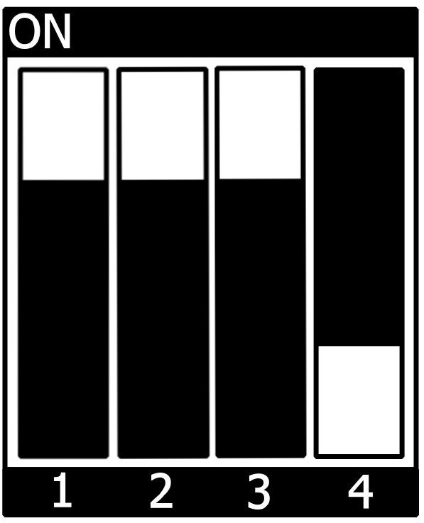
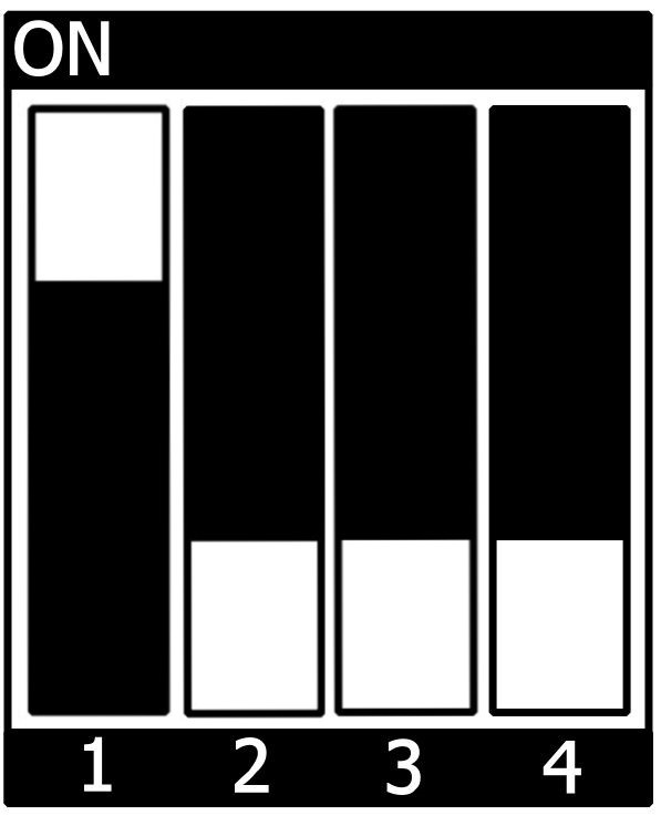
Boot Switch Settings
Boot Mode Design Considerations
Bootpin voltages have to be valid when X_nRESET is released.
System Reset (S1)
The phyBOARD-Sargas is equipped with a System Reset switch at S1 (push button).
Pressing this switch will toggle the X_nRESET pin (X1 Pin D51) of the phyCORE‑STM32MP15x, to Low state, causing the module to reset with a complete power cycle.
System ON/OFF/Wake-up (S2)
The phyBOARD-Sargas is equipped with an ON/OFF/Wake-up switch at S2 (push button).
Pressing this switch will toggle the X_nPONKEY pin (X1 Pin D54) of the phyCORE‑STM32MP15x, to low state. On the phyCORE, this signal is directly connected to the PMIC PONKEYn input pin.
- A long keypress enables powering OFF the system.
- A single keypress enables powering ON the system or waking up from any Low Power mode.
Note
This behavior depends on the BSP configuration. More information can be found in the STM32MP15x and STPMIC1A datasheets.
User Programmable Switches (S4, S5)
The phyBOARD-Sargas is equipped with two User Programmable Switches S4, and S5 (push buttons).
Those switches allow any Software application to used it as an event source :
- Pressing S4 switch will toggle to X_DBTRGO/PA13 Low state (on the phyCORE‑STM32MP15x, it will light up LED red D2).
- Pressing S5 switch will toggle to X_DBTRGI/PA14 Low state (on the phyCORE‑STM32MP15x, it will light up LED green D1).
Additional System Level Hardware Information
Soldering Jumpers and 0 Ohm resistors
Numerous soldering jumpers and 0 Ohm resistors allow the phyBOARD-Sargas to be configured according to various application needs.
Soldering Jumpers
| Reference | Position | Description | Section |
|---|---|---|---|
| J2 | 1+2 | Audio Jack/Headset detection: dc coupling | Audio Connectivity (X5, X26, X27, X28) |
| 2+3 | Audio Jack/Headset detection: capless application | ||
| J3 | 1+2 | CAM_MCLK from X_MCO2/PG2 pin | Camera Connectivity (X4) |
| 2+3 | CAM_MCLK from 27MHz oscillator (OZ1) | ||
| J4 | 1+2 | CAM_CTRL2 to GND | Camera Connectivity (X4) |
| 2+3 | CAM_CTRL2 to VCC_CAM | ||
| not mounted | CAM_CTRL2 not connected | ||
| J5 | 1+2 | CAM_CTRL1 to GND | Camera Connectivity (X4) |
| 2+3 | CAM_CTRL1 to VCC_CAM | ||
| J7 | 1+2 | X_nRESET to X24 | Audio/Visual Connectors (X24 and X25) |
| 2+3 | X_LCD_RST/PD9 to X24 | ||
| J8 | 1+2 | I2C address of STMPE811 (U20) = 0x41 | Audio Connectivity (X5, X26, X27, X28) |
| 2+3 | I2C address of STMPE811 (U20) = 0x44 | ||
J9 | closed | GND connected to AGND via a star point | Audio Connectivity (X5, X26, X27, X28) |
J10 | closed | GND connected to AGND via a star point | Audio Connectivity (X5, X26, X27, X28) |
| J17 | 1+2 | X_SAI2_SCK_B/PH2 connected to X24 | Audio/Visual Connectors (X24 and X25) |
| 2+3 | X_SPI16_SCK/PZ0 connected to X24 | ||
| J18 | 1+2 | X_SAI2_FS_B/PC0 connected to X24 | Audio/Visual Connectors (X24 and X25) |
| 2+3 | X_SPI16_NSS/PZ3 connected to X24 | ||
| J19 | 1+2 | X_SAI2_SD_A/PI6 connected to X24 | Audio/Visual Connectors (X24 and X25) |
| 2+3 | X_SPI16_MISO/PZ1 connected to X24 | ||
| J20 | 1+2 | X_SAI2_SD_B/PF11 connected to X24 | Audio/Visual Connectors (X24 and X25) |
| 2+3 | X_SPI16_MOSI/PZ2 connected to X24 | ||
| J21 | 1+2 | X_SAI2_SCK_B/PH2 connected to X7 | Raspberry Pi HAT Connectivity (X7) |
| 2+3 | TIM1_CH2/PE11 (X_LCD_G3/PE11) connected to X7 | ||
| J22 | 1+2 | X_PH5 connected to X7 | Raspberry Pi HAT Connectivity (X7) |
| 2+3 | TIM1_CH2/PE11 (X_LCD_G3/PE11) connected to X7 | ||
| J23 | 1+2 | X_USB_OTG_D2M connected to X12 | Universal Serial Bus USB Connectivity (X2, X12) ----- Expansion Connector (X33) |
| 2+3 | X_USB_OTG_D2M connected to X33 | ||
| J24 | 1+2 | X_USB_OTG_D2P connected to X12 | Universal Serial Bus USB Connectivity (X2, X12) ----- Expansion Connector (X33) |
| 2+3 | X_USB_OTG_D2P connected to X33 | ||
| J29 | 1+2 | TPS62150 Step-Down Converter (U5) disabled | Camera Connectivity (X4) |
| 2+3 | TPS62150 Step-Down Converter (U5) enabled | ||
J35 | 1+2 | X_PF2 connected to X7 | Raspberry Pi HAT Connectivity (X7) |
| 2+3 | X_DACOUT2_TIM8_CH1N/PA5 connected to X7 | ||
J36 | 1+2 | TIM12_CH2/PH9 (X_DCMI_DATA0/PH9) connected to X3 | Arduino Shields Connectivity (X3) |
| 2+3 | X_DFSDM1_CKOUT/PD10 connected to X3 | ||
| J37 | 1+2 | X_PG8 connected to X3 | Arduino Shields Connectivity (X3) |
| 2+3 | X_SPI16_NSS/PZ3 connected to X3 | ||
J38 | 1+2 | X_TIM15_CH1N/PE4 connected to X3 | Arduino Shields Connectivity (X3) |
| 2+3 | X_SPI16_MOSI/PZ2 connected to X3 | ||
| J39 | 1+2 | Audio Codec (U1) nRESET pin connected to Ground (U1 disabled) | Audio Connectivity (X5, X26, X27, X28) |
| 2+3 | Audio Codec (U1) nRESET pin connected to X_nRESET (U1 enabled) |
Soldering Jumpers Descriptions
0 Ohm Resistors
Those resistors have no functional impact and should be always mounted. Most of the phyBOARD-Sargas TIMERs signals are alternate functions of X_LCD_x or X_DCMI_x signals (configured by Software Pin muxing in the BSP). For better schematic visibility and to avoid any signal length routing issue when using LCD or DCMI function, 0 Ohm resistors are mounted by default between X_LCD or X_DCMI and TIMx_CHy signals. Additionally, two X_DFSDM signals are used as ADC on the phyBOARD, so the same logic has been done for those two signals.
| Reference | Populated | Description | Section |
|---|---|---|---|
| R228 | mounted | TIM8_CH1/PI5 connected to PI5 MPU pin (= X_LCD_B5/PI5) | Motor Control Connector (X38) |
| not mounted | TIM8_CH1/PI5 Not connected to PI5 MPU pin | ||
| R230 | mounted | TIM8_CH2/PC7 connected to PC7 MPU pin (= X_DCMI_DATA1/PC7) | Motor Control Connector (X38) |
| not mounted | TIM8_CH2/PC7 Not connected to PC7 MPU pin | ||
| R231 | mounted | TIM8_CH2N/PB0 connected to PB0 MPU pin (= X_LCD_R3/PB0) | Motor Control Connector (X38) |
| not mounted | TIM8_CH2N/PB0 Not connected to PB0 MPU pin | ||
| R232 | mounted | TIM8_CH3N/PH15 connected to PH15 MPU pin (= X_LCD_G4/PH15) | Motor Control Connector (X38) |
| not mounted | TIM8_CH3N/PH15 Not connected to PH15 MPU pin | ||
| R234 | mounted | ADC2_INP2/PF13 connected to PF13 MPU pin (= X_DFSDM1_DATIN3/PF13) | Arduino Shields Connectivity (X3) |
| not mounted | ADC2_INP2/PF13 Not connected to PF13 MPU pin | ||
| R238 | mounted | ADC1_INP13_INN12/PC3 connected to PC3 MPU pin (= X_DFSDM1_DATIN1/PC3) | Arduino Shields Connectivity (X3) |
| not mounted | ADC1_INP13_INN12/PC3 Not connected to PC3 MPU pin | ||
| R239 | mounted | TIM8_CH3/PI7 connected to PI7 MPU pin (= X_DCMI_DATA7/PI7) | Motor Control Connector (X38) |
| not mounted | TIM8_CH3/PI7 Not connected to PI7 MPU pin | ||
| R240 | mounted | TIM1_CH2/PE11 connected to PE11 MPU pin (= X_LCD_G3/PE11) | Raspberry Pi HAT Connectivity (X7) ----- Motor Control Connector (X38) |
| not mounted | TIM1_CH2/PE11 Not connected to PE11 MPU pin | ||
| R241 | mounted | TIM4_CH2/PB7 connected to PB7 MPU pin (= X_DCMI_VSYNC/PB7) | Arduino Shields Connectivity (X3) |
| not mounted | TIM4_CH2/PB7 Not connected to PB7 MPU pin | ||
| R242 | mounted | TIM15_CH1/PE5 connected to PE5 MPU pin (= X_DCMI_DATA6/PE5) | Arduino Shields Connectivity (X3) |
| not mounted | TIM15_CH1/PE5 Not connected to PE5 MPU pin | ||
| R244 | mounted | TIM12_CH2/PH9 connected to PH9 MPU pin (= X_DCMI_DATA0/PH9) | Arduino Shields Connectivity (X3) |
| not mounted | TIM12_CH2/PH9 Not connected to PH9 MPU pin | ||
| R245 | mounted | TIM5_CH1/PH10 connected to PH10 MPU pin (= X_LCD_R4/PH10) | Motor Control Connector (X38) |
| not mounted | TIM5_CH1/PH10 Not connected to PH10 MPU pin | ||
| R246 | mounted | TIM5_CH4/PI0 connected to PI0 MPU pin (= X_LCD_BL_PWM/PI0) | Motor Control Connector (X38) |
| not mounted | TIM5_CH4/PI0 Not connected to PI0 MPU pin | ||
| R249 | mounted | TIM5_CH3/PH12 connected to PH12 MPU pin (= X_LCD_R6/PH12) | Motor Control Connector (X38) |
| not mounted | TIM5_CH3/PH12 Not connected to PH12 MPU pin | ||
| R270 | mounted | TIM3_CH1/PA6 connected to PA6 MPU pin (= X_DCMI_PIXCLK/PA6) | Motor Control Connector (X38) |
| not mounted | TIM3_CH1/PA6 Not connected to PA6 MPU pin |
0 Ohm Resistor Descriptions
Due to the small footprint of the jumpers / 0 Ohm resistors, we do not recommend manual jumper/resistor modifications. This may render the warranty invalid. Please contact our sales team if you need one of the configurations described below.
I2C Connectivity
I2C4 Interface
The I2C4 interface is intended to be used for the SOM only. But the interface is available on the SOM connector:
pin X1.D21 = X_I2C4_SCL/PZ4 and pin X1.D22 = X_I2C4_SDA/PZ5
This bus is also used for security purposes. This is why on the phyBOARD, the Crypto AuthentificationATECC508A device (U24) is connected to this I2C4 bus at address 0x60. Otherwise, this bus is not available on phyBOARD-Sargas expansion connectors.
I2C1 Interface
The I2C1 interface is intended to be used for the phyBOARD only (not used on the SOM). The table below provides a list of the expansions connectors and pins with I2C1 connectivity
Connector | Connector Pin # | Signal name | Jumper setting |
|---|---|---|---|
| X20 | 6 | X_I2C1_SCL/PF14 | |
| 8 | X_I2C1_SDA/PF15 | ||
| X24 | 15 | X_I2C1_SCL/PF14 | |
| 16 | X_I2C1_SDA/PF15 | ||
| X3 | 17 | X_I2C1_SDA/PF15 | JP27/JP28 1+2 |
| 18 | X_I2C1_SCL/PF14 | JP28/JP28 1+2 | |
| X7 | 3 | X_I2C1_SDA/PF15 | |
| 5 | X_I2C1_SCL/PF14 | ||
| 27 | X_I2C1_SDA/PF15 | ||
| 28 | X_I2C1_SCL/PF14 | ||
| X33 | 11 | X_I2C1_SDA/PF15 | |
| 13 | X_I2C1_SCL/PF14 | ||
| X41 | 21, 22 | X_I2C1_SCL/PF14 | |
| 23, 24 | X_I2C1_SDA/PF15 |
I2C1 Interface Pin Locations
I2C5/I2C6 Interface (possible additional I2C interface)
I2C5 (or I2C6) is a possible additional I2C interface that is available on expansion connectors (X3 or X7), in case X_USART1_CTS/PA11 and X_USART1_RTS/PA12 signals are not used for USART1 flow control. In this case, the pin muxing (BSP) must be changed to configure those signals as an I2C bus. The table below provides a list of the expansions connectors and pins with I2C5/I2C6 connectivity:
Connector | Connector Pin # | Signal name | Jumper Setting |
|---|---|---|---|
| X3 | 17 | X_USART1_RTS/PA12 (I2C56_SDA) | JP27/JP28 2+3 |
| 18 | X_USART1_CTS/PA11 (I2C56_SCL) | JP28/JP28 2+3 | |
| X7 | 11 | X_USART1_RTS/PA12 (I2C56_SDA) | |
| 36 | X_USART1_CTS/PA11 (I2C56_SCL) |
I2C5/I2C6 Interface Pin Locations
If needed, 2K pull-ups can be mounted on the I2C5/I2C6 bus: X_USART1_RTS/PA12 (SDA) with resistor R273 and X_USART1_CTS/PA11 (SCL) with resistor R274.
I2C4 and I2C1 Connectivity
To avoid any conflicts when connecting external I2C devices to the phyBOARD-Sargas, the addresses of the onboard I2C devices must be considered. The table below lists the addresses already in use and shows only the default address. The I²C addresses are hexadecimal in an 8-bit representation. In Linux, a 7-bit representation may be used. In this case, the address value must be shifted one digit to the right. The specification refers to the write address (bit 0 = 0), the read address is increased by 1 according to bit 1 = 1.
Board | Prod. No. | Device | Address used (7 MSB) |
|---|---|---|---|
| I2C4 | |||
phyCORE | PCM-068 | RTC (RV-3028-C7) | 0x52 |
| EEPROM (M24C32) | 0x50 | ||
| PMIC (STPMIC1) | 0x33 and 0x58 | ||
| phyBOARD | PCM-939 | CryptoAuthentication Device (ATECC508A) | 0x60 |
| I2C1 | |||
| phyBOARD | PCM-939 | RGB LED (PCA9533/01) | 0x62 |
| Audio Codec (TLV320AIC3007) | 0x18 | ||
| Resistive Touch driver (STMPE811) | 0x44 by default (J8=2+3) | ||
| AV-Adapter HDMI | PEB-AV-01 | HDMI Core (TDA19988) | 0x70 |
| CEC Core (TDA19988) | 0x34 | ||
| AV-Adapter Display (with 7'' EDT Display) | KPEB-AV-02 | Touchscreen driver (EDT ft5x06) | 0x38 |
I2C Addresses in Use
Warning
Additional I2C devices can be added to the I2C1 bus through the different expansion connectors (with PHYTEC expansion boards or custom boards). In this case, all the I2C device addresses must be unique to avoid conflict.
Revision History
Changes in this manual | Version # | Changes in this manual |
|---|---|---|
|
| Preliminary Manual |
23.02.2022 | L-875e.A1 | Re-release |
29.07.2022 | L-875e.A2 | PDF version |