


 Deutsch
  Englisch
  PHYTEC France
  PHYTEC USA
  PHYTEC India
  PHYTEC China
 Gesamtbetrag:
zzgl. Mwst.
FPSC Gamma Feature Set Specifications (LAN-118e.A0)
Table of Contents
FPSC Introduction
The footprint of the FPSC module is optimized for size and price and guarantees a particularly high production yield thanks to its highly stable solder joints. FPSC modules have a special pinout divided into three zones: core functionalities are in the center, and special or future processor features can be routed on pins around the outside. With FPSC, you gain flexibility for the future. The pin-compatible modules of a feature set enable product variants and upgrades across processor boundaries - without loss of functionality. To achieve this pin compatibility and to be able to use all PHYTEC modules, the complete feature set footprint must be provided on your baseboard.
FPSC Advantages
- Solder joint geometry ensures maximum ruggedness and force distribution
- Vibration and shock tests according to the EN 60068-2 series of standards confirm robustness
- FTGA soldering technology compensates for coplanar deviations between the module and baseboard
- Bilateral solder reservoirs minimize the risk of faulty solder joints
FPSC Module Universal Footprint
- FPSC is based on feature sets.
- Processors within a feature set are pin-compatible and interchangeable.
- In the core area of the module are the guaranteed features - common features such as Ethernet, USB, PCIe, GPIO, and more.
3 Feature Types
Must-have
All modules in a feature set are supported and provide the necessary interfaces to develop many products.
Preferred Signals
The Preferred Signals pins are routed to pins currently supported by many processors and should be considered for future System on Modules of the FPSC feature set.
Proprietary Signals
The third type allows the use of processor features that are not subject to standardization and is therefore unique to a processor. This allows the use of special and new processor features.
Physical Layer
Module
According to the FPSC specification, no fixed PCB sizes and no fixed aspect ratio for a module are defined for Feature Set FPSC-24A. To achieve pin compatibility and to be able to use all PHYTEC modules, the complete feature set footprint must be provided on your baseboard.
| Outline | Vertical | Horizontal |
|---|---|---|
| Min | 30 mm | 27 mm |
| Max | 53 mm | 50 mm |
Baseboard
Footprints/Soldermask
Design for testing:
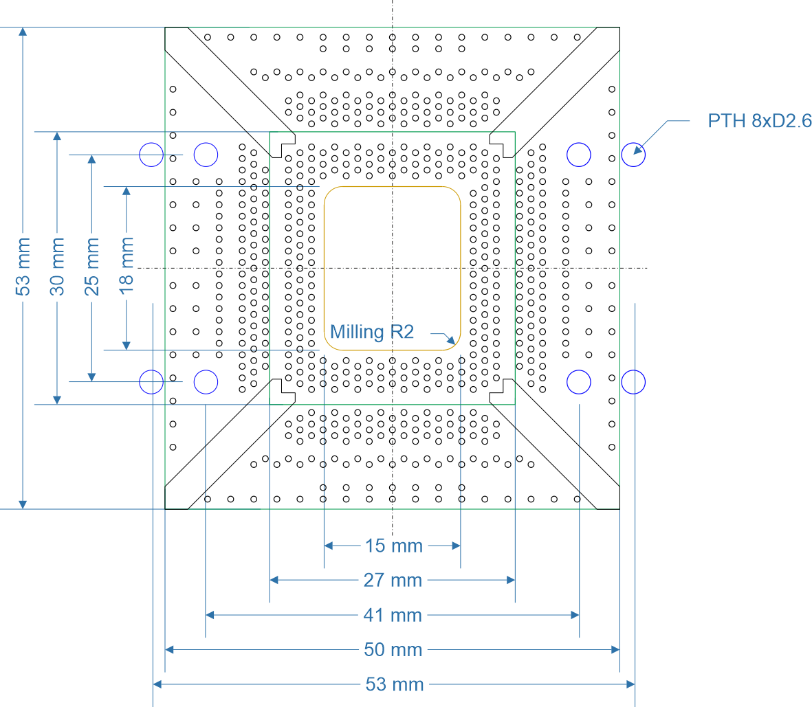
Testing Design
The anchor joints are suitable for attaching a desoldering tool.
Pin Numbering
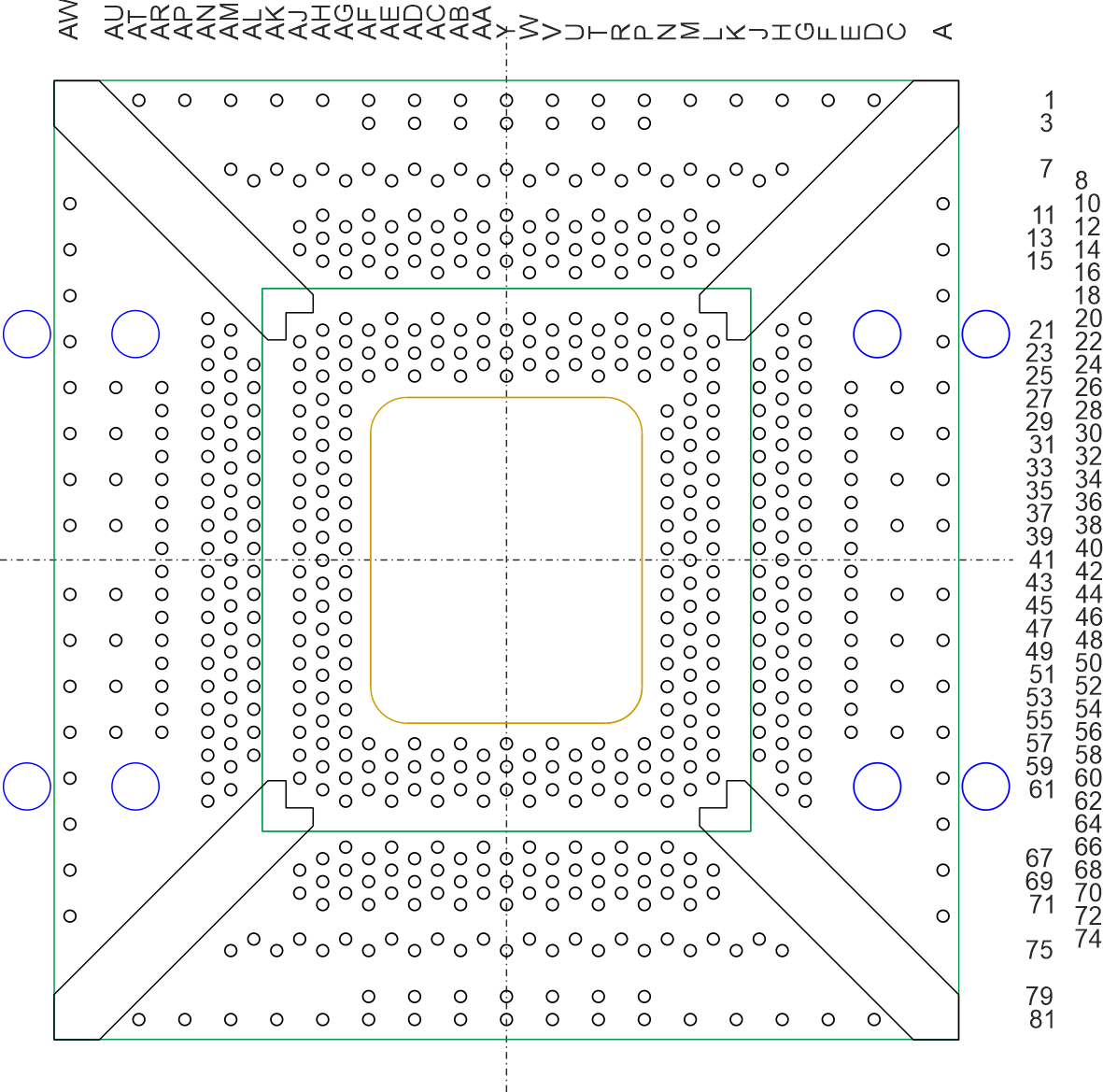
Baseboard - Top View
Thermal Management / Drill Holes
Surface enlargements (i.e. heatspreaders) are individual for each module. FPSC defines the contact surfaces and the fastening of surface enlargement utilizing the metalized holes (Baseboard - Top View). The holes on the baseboard may be omitted (e.g. device-specific heat dissipation concept, fixing to a SOM). PHYTEC surface enlargements use the holes defined above.
Recommended Baseboard PCB Stackup
The following layer structures can be used as a reference for the base board. With these layer structures, 45-50 Ohm single-ended and 85-100 Ohm differential impedance +/- 2 Ohm are possible. At the same time, this layer structure guarantees the fan-out of the module.
6 Layer
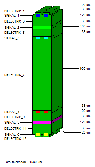
PCB Stackup - 6 Layer
8 Layer
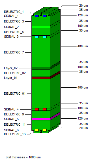
PCB Stackup - 8 Layer
Electrical Layer
Operating Ground / GND
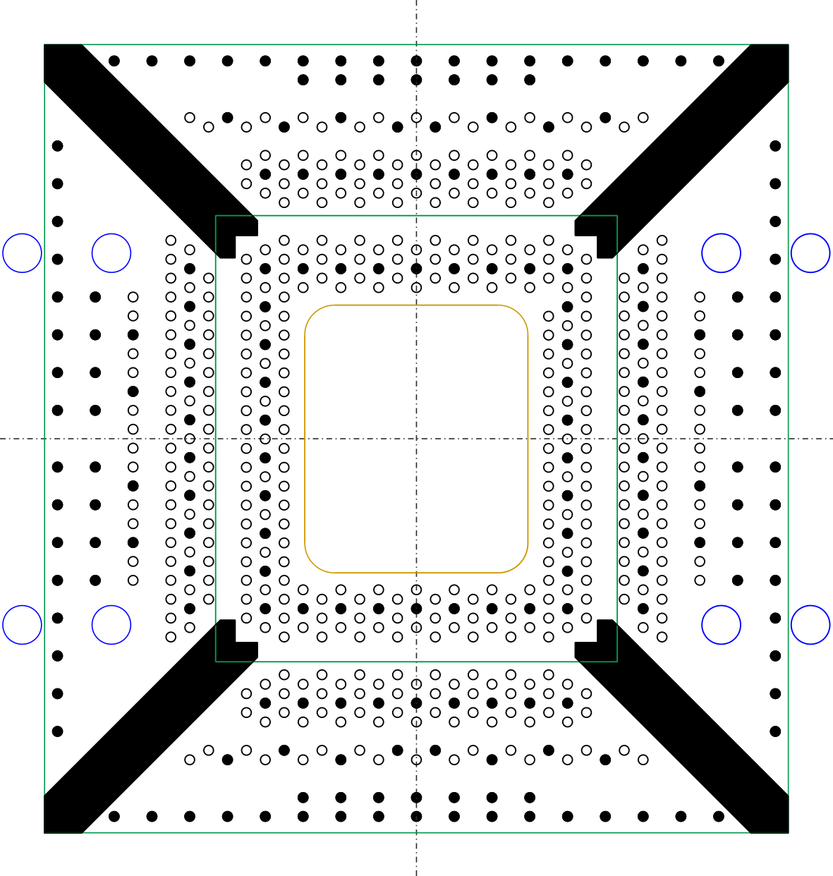
Operating Ground Pins
Operating ground pins/GND are marked black in the picture. In addition to the retaining pads, these are the following pins:
| Zone | Pin Number |
|---|---|
| 1 | M23, P23, T23, V23, Y23, AB23, AD23, AF23, AH23, AH27, AH31, AH35, AH39, AH43, AH47, AH51, AH55, AH59, AF59, AD59, AB59, Y59, V59, T59, P59, M59, M55, M51, M47, M43, M39, M35, M31, M27 |
| 2 | M13, P13, T13, V13, Y13, AB13, AD13, AF13, AH13, AM23, AM27, AM31, AM35, AM39, AM43, AM47, AM51, AM55, AM59, AH69, AF69, AD69, AB69, Y69, V69, T69, P69, M69, H59, H55, H51, H47, H43, H39, H35, H31, H27, H23 |
| 3 | K7, N8, T7, W8, AA8, AD7, AG8, AK7, AR30, AR36, AR46, AR52, AK75, AG74, AD75, AA74, W74, T75, N74, K75, E52, E46, E36, E30 |
| 4 | P3, T3, V3, Y3, AB3, AD3, AF3, AU26, AU30, AU34, AU38, AU44, AU48, AU52, AU56, D1, F1, H1, K1, M1, P1, T1, V1, Y1, AB1, AD1, AF1, AH1, AK1, AM1, AP1, AT1, AW10, AW14, AW18, AW22, AW26, AW30, AW34, AW38, AW44, AW48, AW52, AW56, AW60, AW64, AW68, AW72, AF79, AD79, AB79, Y79, V79, T79, P79, C56, C52, C48, C44, C38, C34, C30, C26, AT81, AP81, AM81, AK81, AH81, AF81, AD81, AB81, Y81, V81, T81, P81, M81, K81, H81, F81, D81, A72, A68, A64, A60, A56, A52, A48, A44, A38, A34, A30, A26, A22, A18, A14, A10 |
Electrical Characteristics
Recommended Operation Conditions
| Parameter | Min | Max | Unit | |
| Supply Voltage | VCC | 4.75 | 5.25 | V |
| Supply Current | ICC | - | 2.5 | A |
| Logic High-level input voltage | VIH | 1.71 | - | V |
| Logic Low-level input voltage | VIL | - | 0.8 | V |
| Logic High-level output voltage | VOH | 1.71 | - | V |
| Logic Low-level output voltage | VOL | - | 0.8 | V |
Switching Characteristics
| Parameter | Min | Max | Unit | |
| nRESET_OUT after Power-On | tON-ROUT | >0 | - | ms |
| Release nRESET_OUT after nPWRREADY_OUT | tPR-ROUT | >0 | - | ms |
| Release nRESET_OUT after nRESET_IN | tRIN-ROUT | >0 | - | ms |
| Minimum nRESET_IN low time | tRIN_LOW | >0 | - | ms |
| Minimum nPWRREADY_OUT High-Z time | tPR_HZ | >0 | - | ms |
Power Sequencing
All PHYTEC modules have an internal power management system (PMIC) that controls the individual processor voltages and control signals. Complex processors can go into unpredictable states if their power sequencing is incorrect. It is therefore imperative that the specified power sequencing is not affected.
Power-up
All PHYTEC modules start power-up sequencing automatically after the supply voltage is applied. To simplify the design-in, the power-up in PHYTEC modules is optimized for three control lines:
- nPWRREADY_OUT (Pin U22)
- nRESET_OUT (Pin R22)
- nRESET_IN (Pin Y21)
nPWRREADY_OUT is an open-drain output on the module and requires an external pull-up resistor (<12V). nPWRREADY_OUT is pulled to GND by the SOM when all processor voltages are properly brought up. Once nPWRREADY_OUT is pulled to GND, voltages can be applied to the processor pins (e.g., push-pull outputs and pull-up/pull-down resistors). Use nPWRREADY_OUT to control the power to the peripherals connected to the module on your custom baseboard.
nRESET_OUT is an open-drain output on the module with an internal pull-up resistor (1.8 V). nRESET is held to GND during power sequencing. After nPWRREADY_OUT is also pulled to GND, nRESET_OUT may held to GND for several microseconds. All baseboard peripheral voltages must have ramped up during this time. If it takes more time for these voltages to ramp up, nRESET_IN can be held at GND on the baseboard for as long as necessary. Once nRESET_OUT is switched to high impedance, the processor will begin the boot process. You should connect nRESET_OUT to the reset inputs of your baseboard peripherals. nRESET_OUT is not intended to perform a CPU reset! Use nRESET_IN (Pin Y21) instead (see below).
nRESET_IN is an open-drain input on the module with an internal pull-up resistor (1.8 V). nRESET_IN is intended to perform a CPU reset. On falling edge and depending on the module, the module will cycle some or all module power rails to reset the module properly. In this case, nPWRREADY_OUT may switch to a High-Z state as described above. nRESET_IN can be used to delay the boot process by holding it on GND during power-up. After Power-up and on rising edge the the processor will begin the boot process.
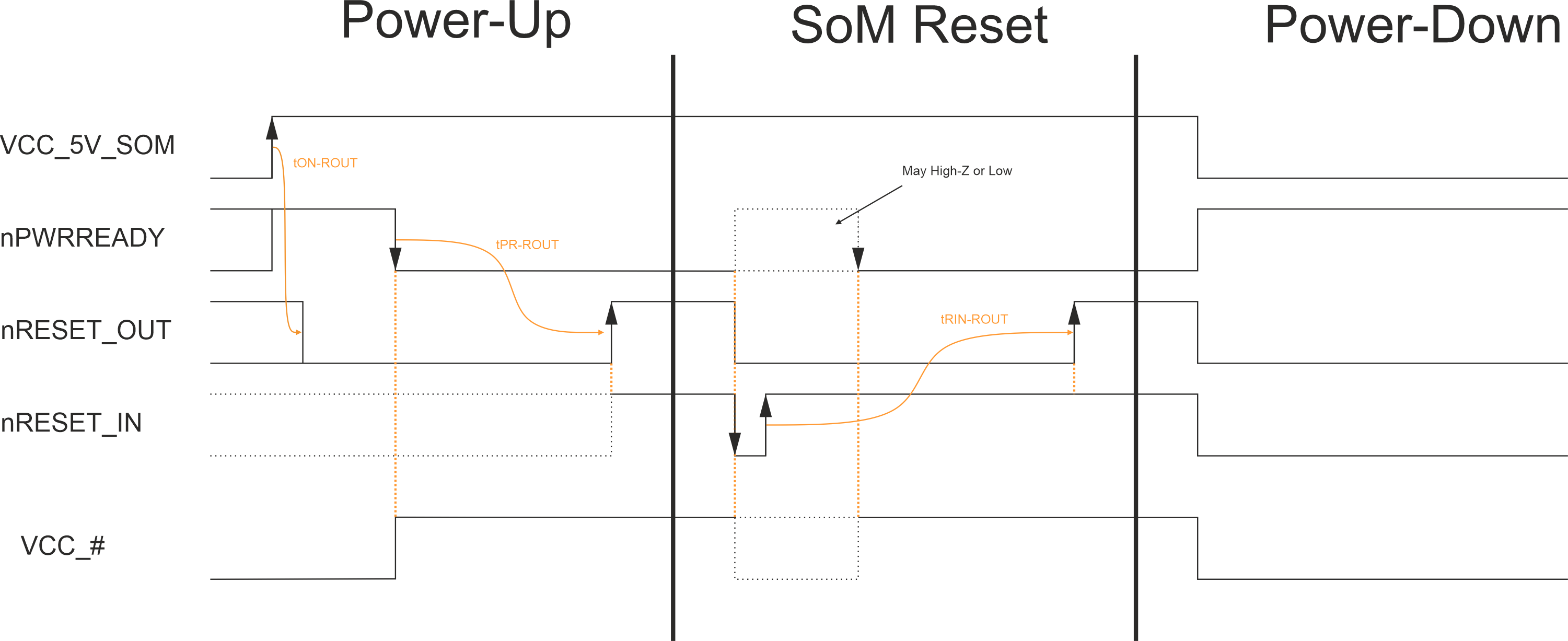
VCC_5V_SOM: SOM Supply Voltage
nPWRREADY_OUT: SOM Open-Drain Output. An external Pullup is needed. See above.
nRESET_OUT: Open-Drain Output, Reset Output for Basboarddevices
nRESET_IN: Open-Drain Input, CPU Reset (State-Controlled) / PWR Reset (on falling edge)
VCC_#: Any perpherial power supply of the baseboard.
When designing power sequencing your baseboard, consider the case of a brief loss of external power. You may be using peripherals that operate with a power-on reset. To ensure that these peripherals are always in a defined state, an additional discharge of the voltages switched via nPWRREADY_OUT is often a useful addition.
Power-cycle / Reset
nRESET_IN (pin Y21) is an open-drain input with an internal pull-up resistor (1.8 V). Use nRESET_IN to trigger a reset or power-cycle the module. You can connect nRESET_IN to a push-button or GPO.
On the falling edge of nRESET_IN, the module starts the reset sequence. nPRWREADY (U22) may be set to HIGH-Z during that.
On the rising edge of nREST_IN the the processor will begin the boot process and nRESET_OUT will be set to a High-Z state.
Boot Source Selection
FPSC provides 4 signals for boot source selection. The signals BOOT_MODE0 (Pin AA4), BOOT_MODE1 (Pin AA5), BOOT_MODE2 (Pin AA6), and BOOT_MODE3 (Pin AA7) are usually connected directly to the processor. The boot mode is evaluated by the processor in relation to the rising nRESET edge. If the signals for boot source selection on the baseboard are not connected (open), an internal mass storage device is set as the default boot source for the user-stage bootloader.
Possible boot sources for the user-stage bootloader could be:
- (SOM) internal NOR-Flash
- (SOM) internal eMMC
- (SOM) internal Bootfuses (referring to another boot source)
- SD-Card
- Ethernet
- USB-Serial
- USB-Mass Storage
- UART
If an interface is available more than once, at least the first interface can always be used as the boot source. The user-stage bootloader may provide additional options for loading the operating system (e.g. kernel and file system).
Interfaces
All signals refer to 1.8V IO voltage unless otherwise noted.
If an interface exists more than once, they are numbered starting from 1. The ordering is determined by
- Bootability, boot source first.
- The maximum achievable data rate of the interface, starting with the fastest.
SD-Card Interface
The module provides the power supply for the SD card. The interface allows various “bus speed modes” that the SD card can negotiate with the host processor. The logic voltage may be 3.3 V or 1.8 V depending on the SD card used. No additional circuitry is required on the baseboard (except capacitors for VCC) as the module implements the logic for this. The CD and WP signals have an internal pull-up.
CAN(-FD) Interface
You can always rely on a CAN interface. If a processor supports CAN-FD, it can be used on the baseboard with an appropriate transceiver. Due to its backward compatibility, CAN-FD can also be used in a CAN system.
UART
There are 3 UART interfaces with different prioritization.
- Primary Debug Interface for debug outputs of the main CPU
- Special Debug Interface for debug outputs of the support CPU (if available)
- A normal UART interface with no special function for the baseboard
All UARTs work as DTE (TxD and RTS are outputs, RxD and CTS are inputs). Under certain circumstances, the signal direction can be reversed within the CPU. You can find more information on this in the processor data sheet.
Pinout
| Must-Have-Signal |
| Preferred-Signal |
| Proprietary-Signal |
| Test-Signal |
The signal direction is defined from the module's point of view.
PWR/CTRL
| FPSC24 Pin Number | FPSC24 Primary Function | I/O | Recommendation |
|---|---|---|---|
| P25 | BOOT_MODE1 | IN | Use <=1kOhm PU (1.8 V) or PD resistors on the baseboard to select the boot source. Consider the HW Manual sheet for valid boot modes. |
| R24 | BOOT_MODE2 | IN | Use <=1kOhm PU (1.8 V) or PD resistors on the baseboard to select the boot source. Consider the HW Manual sheet for valid boot modes. |
| T25 | BOOT_MODE3 | IN | Use <=1kOhm PU (1.8 V) or PD resistors on the baseboard to select the boot source. Consider the HW Manual sheet for valid boot modes. |
| U24 | BOOT_MODE4 | IN | Use <=1kOhm PU (1.8 V) or PD resistors on the baseboard to select the boot source. Consider the HW Manual sheet for valid boot modes. |
| AD21 | JTAG_Reserved | - | JTAG-Bus |
| AC20 | JTAG_TCK | IN | JTAG-Bus |
| AC22 | JTAG_TDI | IN | JTAG-Bus |
| AD25 | JTAG_TDO | OUT | JTAG-Bus |
| AC24 | JTAG_TMS | IN | JTAG-Bus |
| U22 | nPWRREADY_OUT | OD_OUT | Needs an external PU-Resistor (abs. max. 12 V). Use it to control the power sequencing of your baseboard. See Powersequencing. |
| Y21 | nRESET_IN | OD_IN | Internal PU-Resistor. Once it is asserted low, the Module performs a cold reset/power cycle. Intended to connect a push-button. See Powersequencing. |
| R22 | nRESET_OUT | OD_OUT | Internal PU-Resistor. This pin is internally connected to the processor and the PMIC. It is recommended to use this pin only as an output. Connect it to the reset input of your baseboard peripherals. See Powersequencing. |
| R20 | ON/OFF | IN | Internal PU-Resistor. Wake up and power off the Processor. Intended to connect a push-button. Refer to Processors Datasheet for further information. |
| V21 | PMIC_ON_REQUEST | OUT | When it is asserted high, the Module starts power on sequence. This pin is connected internally to the processor and the PMIC. It is recommended not to connect it. Refer to Processors Datasheet for further information. |
| W20 | PMIC_STANDBY_REQUEST | OUT | When it is asserted high, PMIC enters STANDBY mode. This pin is connected internally to the processor and the PMIC. It is recommended not to connect it. Refer to Processors Datasheet for further information. |
| V25 | Reserved for future use | - | For future use |
| W22 | Reserved for future use | - | For future use |
| W24 | Reserved for future use | - | For future use |
| N28 | Reserved for future use | - | For future use |
| P15 | Reserved for future use | - | For future use |
| U20 | RTC_CLKOUT | OUT | 3.3 V Clock-Output of Modules RTC |
| T21 | RTC_nINT | OD_OUT | Interrupt-Output of Modules RTC. Needs external PU-Resistor. |
| AA20 | VCC_1V8_OUT1 | PWR_OUT | Voltage Output for general use (min. 200 mA) |
| AB21 | VCC_1V8_OUT2 | PWR_OUT | Voltage Output for general use (min. 200 mA) |
| AA24 | VCC_3V3_OUT1 | PWR_OUT | Voltage Output for general use (min. 200 mA) |
| AB25 | VCC_3V3_OUT2 | PWR_OUT | Voltage Output for general use (min. 200 mA) |
| L24 | VCC_IN1 | PWR_IN | 5V-DC |
| M25 | VCC_IN2 | PWR_IN | 5V-DC |
| N24 | VCC_IN3 | PWR_IN | 5V-DC |
| L22 | VCC_IN4 | PWR_IN | 5V-DC |
| N22 | VCC_IN5 | PWR_IN | 5V-DC |
| M21 | VCC_IN6 | PWR_IN | 5V-DC |
| N20 | VCC_IN7 | PWR_IN | 5V-DC |
| P21 | VCC_IN8 | PWR_IN | 5V-DC |
| AA22 | VCC_RTC | PWR_IN | Connect a gold cap or a battery here. If a battery is used, make sure that the RTC trickle charger is deactivated! |
| Y25 | Reserved for future use | - | For future use |
GPIO/PWM
| FPSC24 Pin Number | FPSC24 Primary Function | I/O | Recommendation |
|---|---|---|---|
| AL32 | GPIO1 | I/O | |
| AN30 | GPIO2 | I/O | |
| AN32 | GPIO3 | I/O | |
| L40 | GPIO4 | I/O | |
| N40 | GPIO5 | I/O | |
| AL34 | GPIO6 | I/O | |
| AN34 | GPIO7 | I/O | |
| N48 | PWM1 | OUT | |
| N58 | PWM2 | OUT | |
| AL42 | PWM3 | OUT | |
| AN52 | PWM4 | OUT |
10Gb-Ethernet
| FPSC24 Pin Number | FPSC24 Primary Function | I/O | Recommendation |
|---|---|---|---|
| W70 | Reserved for future use | IN | 10G-Ethernet-Bus Intended to connect a 10G Ethernet-PHY. |
| V71 | Reserved for future use | IN | 10G-Ethernet-Bus Intended to connect a 10G Ethernet-PHY. |
| U70 | Reserved for future use | OUT | 10G-Ethernet-Bus Intended to connect a 10G Ethernet-PHY. The coupling capacitors are located on the module |
| T71 | Reserved for future use | OUT | 10G-Ethernet-Bus Intended to connect a 10G Ethernet-PHY. The coupling capacitors are located on the module |
SAI
| FPSC24 Pin Number | FPSC24 Primary Function | I/O | Recommendation |
|---|---|---|---|
| AJ32 | SAI1_MCLK | OUT | Serial Audio Interface |
| AG28 | SAI1_RX_BCLK | IN | Serial Audio Interface |
| AG30 | SAI1_RX_DATA | IN | Serial Audio Interface |
| AG32 | SAI1_RX_SYNC | IN | Serial Audio Interface |
| AH29 | SAI1_TX_BCLK | OUT | Serial Audio Interface |
| AJ28 | SAI1_TX_DATA | OUT | Serial Audio Interface |
| AJ30 | SAI1_TX_SYNC | OUT | Serial Audio Interface |
QSPI
| FPSC24 Pin Number | FPSC24 Primary Function | I/O | Recommendation |
|---|---|---|---|
| AJ24 | QSPI_CE | OUT | Quad-SPI-Bus |
| AG24 | QSPI_CLK | OUT | Quad-SPI-Bus |
| AF21 | QSPI_DATA_0 | I/O | Quad-SPI-Bus |
| AG20 | QSPI_DATA_1 | I/O | Quad-SPI-Bus |
| AG22 | QSPI_DATA_2 | I/O | Quad-SPI-Bus |
| AH21 | QSPI_DATA_3 | I/O | Quad-SPI-Bus |
| AJ22 | QSPI_DQS | OUT | Quad-SPI-Bus |
ADC
| FPSC24 Pin Number | FPSC24 Primary Function | I/O | Recommendation |
|---|---|---|---|
| R16 | ADC0 | A_IN | Analog-to-Digital-Converter - Do not exceed 1.8 V! |
| T15 | ADC1 | A_IN | Analog-to-Digital-Converter - Do not exceed 1.8 V! |
| U16 | ADC2 | A_IN | Analog-to-Digital-Converter - Do not exceed 1.8 V! |
| U14 | ADC3 | A_IN | Analog-to-Digital-Converter - Do not exceed 1.8 V! |
| V15 | ADC4 | A_IN | Analog-to-Digital-Converter - Do not exceed 1.8 V! |
| W16 | ADC5 | A_IN | Analog-to-Digital-Converter - Do not exceed 1.8 V! |
| W14 | ADC6 | A_IN | Analog-to-Digital-Converter - Do not exceed 1.8 V! |
| Y15 | ADC7 | A_IN | Analog-to-Digital-Converter - Do not exceed 1.8 V! |
SD Card/SDIO
| FPSC24 Pin Number | FPSC24 Primary Function | I/O | Recommendation |
|---|---|---|---|
| V57 | SDCARD_CD | OD_IN | Internal PU-Resistor. |
| W60 | SDCARD_CLK | OUT | |
| W58 | SDCARD_CMD | I/O | |
| W62 | SDCARD_DATA0 | I/O | |
| Y61 | SDCARD_DATA1 | I/O | |
| U60 | SDCARD_DATA2 | I/O | |
| V61 | SDCARD_DATA3 | I/O | |
| Y57 | SDCARD_VCC_OUT | PWR_OUT | internal power supply on SOM (max. 800 mA) |
| V67 | SDCARD_WP | OD_IN | Internal PU-Resistor. |
| J58 | SDIO_CD | OD_IN | |
| H57 | SDIO_CLK | OUT | |
| G56 | SDIO_CMD | I/O | |
| G62 | SDIO_DATA0 | I/O | |
| H61 | SDIO_DATA1 | I/O | |
| G60 | SDIO_DATA2 | I/O | |
| G58 | SDIO_DATA3 | I/O | |
| J56 | SDIO_VIO_OUT | PWR_OUT | |
| G54 | SDIO_WP | OD_IN |
CAN/I2C/I3C/SPI/UART
| FPSC24 Pin Number | FPSC24 Primary Function | I/O | Recommendation |
|---|---|---|---|
| N38 | CAN1_RX | IN | CAN-Bus / CAN-FD-Bus |
| N36 | CAN1_TX | OUT | CAN-Bus / CAN-FD-Bus |
| L38 | CAN2_RX | IN | CAN-Bus / CAN-FD-Bus |
| M37 | CAN2_TX | OUT | CAN-Bus / CAN-FD-Bus |
| L26 | I2C1_SCL_DNU | OD_IO | SOM I2C - Do not connect! |
| L28 | I2C1_SDA_DNU | OD_IO | SOM I2C - Do not connect! |
| L60 | I2C2_SCL | OD_IO | Needs external PU-Resistor. |
| L58 | I2C2_SDA | OD_IO | Needs external PU-Resistor. |
| M61 | I2C3_SCL | OD_IO | Needs external PU-Resistor. |
| N60 | I2C3_SDA | OD_IO | Needs external PU-Resistor. |
| AN36 | I2C4_SCL | OD_IO | Needs external PU-Resistor. |
| AN38 | I2C4_SDA | OD_IO | Needs external PU-Resistor. |
| AN40 | I2C5_SCL/I3C_SCL | OD_IO | Needs external PU-Resistor. I3C if supported by the processor. |
| AN42 | I2C5_SDA/I3C_SDA | OD_IO | Needs external PU-Resistor. I3C if supported by the processor. |
| L34 | SPI1_CS | OUT | |
| N34 | SPI1_MISO | IN | |
| N32 | SPI1_MOSI | OUT | |
| M33 | SPI1_SCLK | OUT | |
| N30 | SPI2_CS | OUT | |
| L32 | SPI2_MISO | IN | |
| L30 | SPI2_MOSI | OUT | |
| M29 | SPI2_SCLK | OUT | |
| AL36 | SPI3_MISO | IN | |
| AL38 | SPI3_MOSI | OUT | |
| AL40 | SPI3_SCLK | OUT | |
| AM41 | SPI3_CS | OUT | |
| M41 | UART1_CTS | IN | |
| N42 | UART1_RTS | OUT | |
| L44 | UART1_RXD | IN | |
| L42 | UART1_TXD | OUT | |
| L46 | UART2_CTS | IN | Special Debug Interface |
| M45 | UART2_RTS | OUT | Special Debug Interface |
| N46 | UART2_RXD | IN | Special Debug Interface |
| N44 | UART2_TXD | OUT | Special Debug Interface |
| AE22 | UART3_RXD | IN | Primary Debug Interface |
| AE20 | UART3_TXD | OUT | Primary Debug Interface |
PCIE
| FPSC24 Pin Number | FPSC24 Primary Function | I/O | Recommendation |
|---|---|---|---|
| AA14 | PCIE1_CLK_N | OUT | PCIe-1-Lane-Bus |
| AB15 | PCIE1_CLK_P | OUT | PCIe-1-Lane-Bus |
| AC16 | PCIE1_nCLKREQ | IN | PCIe-1-Lane-Bus |
| AC14 | PCIE1_nPERST | OUT | PCIe-1-Lane-Bus |
| AB11 | PCIE1_RXN_N | IN | PCIe-1-Lane-Bus |
| AC12 | PCIE1_RXN_P | IN | PCIe-1-Lane-Bus |
| Y11 | PCIE1_TXN_N | OUT | PCIe-1-Lane-Bus |
| AA12 | PCIE1_TXN_P | OUT | PCIe-1-Lane-Bus |
| AL24 | PCIE2_CLK_N | OUT | PCIe-1-Lane-Bus |
| AL26 | PCIE2_CLK_P | OUT | PCIe-1-Lane-Bus |
| AM21 | PCIE2_nCLKREQ | IN | PCIe-1-Lane-Bus |
| AM25 | PCIE2_nPERST | OUT | PCIe-1-Lane-Bus |
| AN26 | PCIE2_RXN_N | IN | PCIe-1-Lane-Bus |
| AN28 | PCIE2_RXN_P | IN | PCIe-1-Lane-Bus |
| AN22 | PCIE2_TXN_N | OUT | PCIe-1-Lane-Bus |
| AN24 | PCIE2_TXN_P | OUT | PCIe-1-Lane-Bus |
LVDS
| FPSC24 Pin Number | FPSC24 Primary Function | I/O | Recommendation |
|---|---|---|---|
| N52 | LVDS1_CLK_N | OUT | LVDS-Display-Interface |
| N50 | LVDS1_CLK_P | OUT | LVDS-Display-Interface |
| L52 | LVDS1_DATA0_N | OUT | LVDS-Display-Interface |
| L50 | LVDS1_DATA0_P | OUT | LVDS-Display-Interface |
| L54 | LVDS1_DATA1_N | OUT | LVDS-Display-Interface |
| M53 | LVDS1_DATA1_P | OUT | LVDS-Display-Interface |
| N56 | LVDS1_DATA2_N | OUT | LVDS-Display-Interface |
| N54 | LVDS1_DATA2_P | OUT | LVDS-Display-Interface |
| M57 | LVDS1_DATA3_N | OUT | LVDS-Display-Interface |
| L56 | LVDS1_DATA3_P | OUT | LVDS-Display-Interface |
| AN54 | LVDS2_CLK_N | OUT | LVDS-Display-Interface |
| AN56 | LVDS2_CLK_P | OUT | LVDS-Display-Interface |
| AN60 | LVDS2_DATA0_N | OUT | LVDS-Display-Interface |
| AM61 | LVDS2_DATA0_P | OUT | LVDS-Display-Interface |
| AL56 | LVDS2_DATA1_N | OUT | LVDS-Display-Interface |
| AL58 | LVDS2_DATA1_P | OUT | LVDS-Display-Interface |
| AM57 | LVDS2_DATA2_N | OUT | LVDS-Display-Interface |
| AN58 | LVDS2_DATA2_P | OUT | LVDS-Display-Interface |
| AL52 | LVDS2_DATA3_N | OUT | LVDS-Display-Interface |
| AL54 | LVDS2_DATA3_P | OUT | LVDS-Display-Interface |
HDMI
| FPSC24 Pin Number | FPSC24 Primary Function | I/O | Recommendation |
|---|---|---|---|
| AJ14 | EARC_N/HDMI_HPD | OUT | HDMI-Interface |
| AH15 | EARC_P/HDMI_UTIL | OUT | HDMI-Interface |
| AH11 | HDMI_CEC | I/O | HDMI-Interface |
| AJ12 | HDMI_HPD | IN | HDMI-Interface |
| AE14 | HDMI_SCL | OD_IO | HDMI-Interface |
| AG14 | HDMI_SDA | OD_IO | HDMI-Interface |
| AD15 | HDMI_TX0_N | OUT | HDMI-Interface |
| AE16 | HDMI_TX0_P | OUT | HDMI-Interface |
| AF11 | HDMI_TX1_N | OUT | HDMI-Interface |
| AG12 | HDMI_TX1_P | OUT | HDMI-Interface |
| AF15 | HDMI_TX2_N | OUT | HDMI-Interface |
| AG16 | HDMI_TX2_P | OUT | HDMI-Interface |
| AD11 | HDMI_TXC_N | OUT | HDMI-Interface |
| AE12 | HDMI_TXC_P | OUT | HDMI-Interface |
DSI
| FPSC24 Pin Number | FPSC24 Primary Function | I/O | Recommendation |
|---|---|---|---|
| AN46 | DSI1_CLK_N | OUT | DSI-Display-Interface |
| AN48 | DSI1_CLK_P | OUT | DSI-Display-Interface |
| AL48 | DSI1_D0_N | OUT | DSI-Display-Interface |
| AL50 | DSI1_D0_P | OUT | DSI-Display-Interface |
| AM49 | DSI1_D1_N | OUT | DSI-Display-Interface |
| AN50 | DSI1_D1_P | OUT | DSI-Display-Interface |
| AN44 | DSI1_D2_N | OUT | DSI-Display-Interface |
| AM45 | DSI1_D2_P | OUT | DSI-Display-Interface |
| AL44 | DSI1_D3_N | OUT | DSI-Display-Interface |
| AL46 | DSI1_D3_P | OUT | DSI-Display-Interface |
CSI
| FPSC24 Pin Number | FPSC24 Primary Function | I/O | Recommendation |
|---|---|---|---|
| R62 | CSI1_CLK_N | IN | CSI-2-(4-Lane)-Bus |
| R60 | CSI1_CLK_P | IN | CSI-2-(4-Lane)-Bus |
| T57 | CSI1_D0_N | IN | CSI-2-(4-Lane)-Bus |
| U58 | CSI1_D0_P | IN | CSI-2-(4-Lane)-Bus |
| T61 | CSI1_D1_N | IN | CSI-2-(4-Lane)-Bus |
| U62 | CSI1_D1_P | IN | CSI-2-(4-Lane)-Bus |
| P57 | CSI1_D2_N | IN | CSI-2-(4-Lane)-Bus |
| R58 | CSI1_D2_P | IN | CSI-2-(4-Lane)-Bus |
| N62 | CSI1_D3_N | IN | CSI-2-(4-Lane)-Bus |
| P61 | CSI1_D3_P | IN | CSI-2-(4-Lane)-Bus |
| H41 | CSI2_CLK_N | IN | CSI-2-(4-Lane)-Bus |
| J42 | CSI2_CLK_P | IN | CSI-2-(4-Lane)-Bus |
| G42 | CSI2_D0_N | IN | CSI-2-(4-Lane)-Bus |
| G44 | CSI2_D0_P | IN | CSI-2-(4-Lane)-Bus |
| J44 | CSI2_D1_N | IN | CSI-2-(4-Lane)-Bus |
| H45 | CSI2_D1_P | IN | CSI-2-(4-Lane)-Bus |
| J38 | CSI2_D2_N | IN | CSI-2-(4-Lane)-Bus |
| J40 | CSI2_D2_P | IN | CSI-2-(4-Lane)-Bus |
| G38 | CSI2_D3_N | IN | CSI-2-(4-Lane)-Bus |
| G40 | CSI2_D3_P | IN | CSI-2-(4-Lane)-Bus |
Ethernet
| FPSC24 Pin Number | FPSC24 Primary Function | I/O | Recommendation |
|---|---|---|---|
| AH57 | GB_ETH1_A_N | I/O | Gb-Ethernet-Interface |
| AJ58 | GB_ETH1_A_P | I/O | Gb-Ethernet-Interface |
| AF57 | GB_ETH1_B_N | I/O | Gb-Ethernet-Interface |
| AG58 | GB_ETH1_B_P | I/O | Gb-Ethernet-Interface |
| AG62 | GB_ETH1_C_N | I/O | Gb-Ethernet-Interface |
| AH61 | GB_ETH1_C_P | I/O | Gb-Ethernet-Interface |
| AE62 | GB_ETH1_D_N | I/O | Gb-Ethernet-Interface |
| AF61 | GB_ETH1_D_P | I/O | Gb-Ethernet-Interface |
| AG60 | GB_ETH1_LED_ACT | Output to sink a LED. Max. Output Low Current 30 mA. Max. Output High Voltage 5 V. | |
| AJ60 | GB_ETH1_LED_LINK | Output to sink a LED. Max. Output Low Current 30 mA. Max. Output High Voltage 5 V. |
RGMII
| FPSC24 Pin Number | FPSC24 Primary Function | I/O | Recommendation |
|---|---|---|---|
| AH45 | RGMII2_EVENT_IN | IN | |
| AJ44 | RGMII2_EVENT_OUT | OUT | |
| AG46 | RGMII2_MDC | OUT | |
| AG44 | RGMII2_MDIO | I/O | Needs external 2k2 PU-Resistor. |
| AG48 | RGMII2_nINT | IN | Connect to RGMII2 Ethernet-PHY Interrupt-Output. |
| AG54 | RGMII2_RX_CTL | IN | |
| AJ56 | RGMII2_RX_D0 | IN | |
| AJ54 | RGMII2_RX_D1 | IN | |
| AJ52 | RGMII2_RX_D2 | IN | |
| AH53 | RGMII2_RX_D3 | IN | |
| AG56 | RGMII2_RXC | IN | |
| AG50 | RGMII2_TX_CTL | OUT | |
| AJ50 | RGMII2_TX_D0 | OUT | |
| AJ48 | RGMII2_TX_D1 | OUT | |
| AH49 | RGMII2_TX_D2 | OUT | |
| AJ46 | RGMII2_TX_D3 | OUT | |
| AG52 | RGMII2_TXC | OUT |
USB
| FPSC24 Pin Number | FPSC24 Primary Function | I/O | Recommendation |
|---|---|---|---|
| AD61 | USB1_D_N | I/O | USB2-Bus |
| AC62 | USB1_D_P | I/O | USB2-Bus |
| AE60 | USB1_ID | IN | USB2-Bus |
| AE58 | USB1_OC | IN | USB2-Bus |
| AD57 | USB1_PWR_EN | OUT | USB2-Bus |
| AF67 | USB1_RX0_N | IN | USB3-Bus |
| AE66 | USB1_RX0_P | IN | USB3-Bus |
| AH67 | Reserved for future use | IN | USB3-Bus |
| AG66 | Reserved for future use | IN | USB3-Bus |
| AF71 | USB1_TX0_N | OUT | USB3-Bus |
| AE70 | USB1_TX0_P | OUT | USB3-Bus |
| AH71 | Reserved for future use | OUT | USB3-Bus |
| AG70 | Reserved for future use | OUT | USB3-Bus |
| AC60 | USB1_VBUS | PWR_IN | USB2-Bus |
| AB61 | USB2_D_N | I/O | USB2-Bus |
| AA62 | USB2_D_P | I/O | USB2-Bus |
| AA60 | USB2_ID | IN | USB2-Bus |
| AC58 | USB2_OC | IN | USB2-Bus |
| AB57 | USB2_PWR_EN | OUT | USB2-Bus |
| AC66 | USB2_RX0_N | IN | USB3-Bus |
| AB67 | USB2_RX0_P | IN | USB3-Bus |
| AA66 | Reserved for future use | IN | USB3-Bus |
| Y67 | Reserved for future use | IN | USB3-Bus |
| AC70 | USB2_TX0_N | OUT | USB3-Bus |
| AB71 | USB2_TX0_P | OUT | USB3-Bus |
| AA70 | Reserved for future use | OUT | USB3-Bus |
| Y71 | Reserved for future use | OUT | USB3-Bus |
| AA58 | USB2_VBUS | PWR_IN | USB2-Bus |
GND
| FPSC24 Pin Number | FPSC24 Primary Function | I/O | Recommendation |
|---|---|---|---|
| A10 | 0V GND | - | Ground |
| A14 | 0V GND | - | Ground |
| A18 | 0V GND | - | Ground |
| A22 | 0V GND | - | Ground |
| A26 | 0V GND | - | Ground |
| A30 | 0V GND | - | Ground |
| A34 | 0V GND | - | Ground |
| A38 | 0V GND | - | Ground |
| A44 | 0V GND | - | Ground |
| A48 | 0V GND | - | Ground |
| A52 | 0V GND | - | Ground |
| A56 | 0V GND | - | Ground |
| A60 | 0V GND | - | Ground |
| A64 | 0V GND | - | Ground |
| A68 | 0V GND | - | Ground |
| A72 | 0V GND | - | Ground |
| D81 | 0V GND | - | Ground |
| F81 | 0V GND | - | Ground |
| H81 | 0V GND | - | Ground |
| K81 | 0V GND | - | Ground |
| M81 | 0V GND | - | Ground |
| P81 | 0V GND | - | Ground |
| T81 | 0V GND | - | Ground |
| V81 | 0V GND | - | Ground |
| Y81 | 0V GND | - | Ground |
| AB81 | 0V GND | - | Ground |
| AD81 | 0V GND | - | Ground |
| AF81 | 0V GND | - | Ground |
| AH81 | 0V GND | - | Ground |
| AK81 | 0V GND | - | Ground |
| AM81 | 0V GND | - | Ground |
| AP81 | 0V GND | - | Ground |
| AT81 | 0V GND | - | Ground |
| C26 | 0V GND | - | Ground |
| C30 | 0V GND | - | Ground |
| C34 | 0V GND | - | Ground |
| C38 | 0V GND | - | Ground |
| C44 | 0V GND | - | Ground |
| C48 | 0V GND | - | Ground |
| C52 | 0V GND | - | Ground |
| C56 | 0V GND | - | Ground |
| P79 | 0V GND | - | Ground |
| T79 | 0V GND | - | Ground |
| V79 | 0V GND | - | Ground |
| Y79 | 0V GND | - | Ground |
| AB79 | 0V GND | - | Ground |
| AD79 | 0V GND | - | Ground |
| AF79 | 0V GND | - | Ground |
| E30 | 0V GND | - | Ground |
| E36 | 0V GND | - | Ground |
| E46 | 0V GND | - | Ground |
| E52 | 0V GND | - | Ground |
| K75 | 0V GND | - | Ground |
| N74 | 0V GND | - | Ground |
| T75 | 0V GND | - | Ground |
| W74 | 0V GND | - | Ground |
| AA74 | 0V GND | - | Ground |
| AD75 | 0V GND | - | Ground |
| AG74 | 0V GND | - | Ground |
| AK75 | 0V GND | - | Ground |
| H23 | 0V GND | - | Ground |
| H27 | 0V GND | - | Ground |
| H31 | 0V GND | - | Ground |
| H35 | 0V GND | - | Ground |
| H39 | 0V GND | - | Ground |
| H43 | 0V GND | - | Ground |
| H47 | 0V GND | - | Ground |
| H51 | 0V GND | - | Ground |
| H55 | 0V GND | - | Ground |
| H59 | 0V GND | - | Ground |
| M69 | 0V GND | - | Ground |
| P69 | 0V GND | - | Ground |
| T69 | 0V GND | - | Ground |
| V69 | 0V GND | - | Ground |
| Y69 | 0V GND | - | Ground |
| AB69 | 0V GND | - | Ground |
| AD69 | 0V GND | - | Ground |
| AF69 | 0V GND | - | Ground |
| AH69 | 0V GND | - | Ground |
| M27 | 0V GND | - | Ground |
| M31 | 0V GND | - | Ground |
| M35 | 0V GND | - | Ground |
| M39 | 0V GND | - | Ground |
| M43 | 0V GND | - | Ground |
| M47 | 0V GND | - | Ground |
| M51 | 0V GND | - | Ground |
| M55 | 0V GND | - | Ground |
| M59 | 0V GND | - | Ground |
| P59 | 0V GND | - | Ground |
| T59 | 0V GND | - | Ground |
| V59 | 0V GND | - | Ground |
| Y59 | 0V GND | - | Ground |
| AB59 | 0V GND | - | Ground |
| AD59 | 0V GND | - | Ground |
| AF59 | 0V GND | - | Ground |
| AH59 | 0V GND | - | Ground |
| AW72 | 0V GND | - | Ground |
| AW68 | 0V GND | - | Ground |
| AW64 | 0V GND | - | Ground |
| AW60 | 0V GND | - | Ground |
| AW56 | 0V GND | - | Ground |
| AW52 | 0V GND | - | Ground |
| AW48 | 0V GND | - | Ground |
| AW44 | 0V GND | - | Ground |
| AW38 | 0V GND | - | Ground |
| AW34 | 0V GND | - | Ground |
| AW30 | 0V GND | - | Ground |
| AW26 | 0V GND | - | Ground |
| AW22 | 0V GND | - | Ground |
| AW18 | 0V GND | - | Ground |
| AW14 | 0V GND | - | Ground |
| AW10 | 0V GND | - | Ground |
| AT1 | 0V GND | - | Ground |
| AP1 | 0V GND | - | Ground |
| AM1 | 0V GND | - | Ground |
| AK1 | 0V GND | - | Ground |
| AH1 | 0V GND | - | Ground |
| AF1 | 0V GND | - | Ground |
| AD1 | 0V GND | - | Ground |
| AB1 | 0V GND | - | Ground |
| Y1 | 0V GND | - | Ground |
| V1 | 0V GND | - | Ground |
| T1 | 0V GND | - | Ground |
| P1 | 0V GND | - | Ground |
| M1 | 0V GND | - | Ground |
| K1 | 0V GND | - | Ground |
| H1 | 0V GND | - | Ground |
| F1 | 0V GND | - | Ground |
| D1 | 0V GND | - | Ground |
| AU56 | 0V GND | - | Ground |
| AU52 | 0V GND | - | Ground |
| AU48 | 0V GND | - | Ground |
| AU44 | 0V GND | - | Ground |
| AU38 | 0V GND | - | Ground |
| AU34 | 0V GND | - | Ground |
| AU30 | 0V GND | - | Ground |
| AU26 | 0V GND | - | Ground |
| AF3 | 0V GND | - | Ground |
| AD3 | 0V GND | - | Ground |
| AB3 | 0V GND | - | Ground |
| Y3 | 0V GND | - | Ground |
| V3 | 0V GND | - | Ground |
| T3 | 0V GND | - | Ground |
| P3 | 0V GND | - | Ground |
| AR52 | 0V GND | - | Ground |
| AR46 | 0V GND | - | Ground |
| AR36 | 0V GND | - | Ground |
| AR30 | 0V GND | - | Ground |
| AK7 | 0V GND | - | Ground |
| AG8 | 0V GND | - | Ground |
| AD7 | 0V GND | - | Ground |
| AA8 | 0V GND | - | Ground |
| W8 | 0V GND | - | Ground |
| T7 | 0V GND | - | Ground |
| N8 | 0V GND | - | Ground |
| K7 | 0V GND | - | Ground |
| AM59 | 0V GND | - | Ground |
| AM55 | 0V GND | - | Ground |
| AM51 | 0V GND | - | Ground |
| AM47 | 0V GND | - | Ground |
| AM43 | 0V GND | - | Ground |
| AM39 | 0V GND | - | Ground |
| AM35 | 0V GND | - | Ground |
| AM31 | 0V GND | - | Ground |
| AM27 | 0V GND | - | Ground |
| AM23 | 0V GND | - | Ground |
| AH13 | 0V GND | - | Ground |
| AF13 | 0V GND | - | Ground |
| AD13 | 0V GND | - | Ground |
| AB13 | 0V GND | - | Ground |
| Y13 | 0V GND | - | Ground |
| V13 | 0V GND | - | Ground |
| T13 | 0V GND | - | Ground |
| P13 | 0V GND | - | Ground |
| M13 | 0V GND | - | Ground |
| AH55 | 0V GND | - | Ground |
| AH51 | 0V GND | - | Ground |
| AH47 | 0V GND | - | Ground |
| AH43 | 0V GND | - | Ground |
| AH39 | 0V GND | - | Ground |
| AH35 | 0V GND | - | Ground |
| AH31 | 0V GND | - | Ground |
| AH27 | 0V GND | - | Ground |
| AH23 | 0V GND | - | Ground |
| AF23 | 0V GND | - | Ground |
| AD23 | 0V GND | - | Ground |
| AB23 | 0V GND | - | Ground |
| Y23 | 0V GND | - | Ground |
| V23 | 0V GND | - | Ground |
| T23 | 0V GND | - | Ground |
| P23 | 0V GND | - | Ground |
| M23 | 0V GND | - | Ground |
| 12 (HOLE) | 0V GND | - | Ground |
| 11 (HOLE) | 0V GND | - | Ground |
| 10 (HOLE) | 0V GND | - | Ground |
| 9 (HOLE) | 0V GND | - | Ground |
| 8 (HOLE) | 0V GND | - | Ground |
| 7 (HOLE) | 0V GND | - | Ground |
| 6 (HOLE) | 0V GND | - | Ground |
| 5 (HOLE) | 0V GND | - | Ground |
| 4 (Anker-Joint) | 0V GND | - | Ground |
| 3 (Anker-Joint) | 0V GND | - | Ground |
| 2 (Anker-Joint) | 0V GND | - | Ground |
| 1 (Anker-Joint) | 0V GND | - | Ground |
Reserved for future use
| FPSC24 Pin Number | FPSC24 Primary Function | I/O | Recommendation |
|---|---|---|---|
| E26 | Reserved for future use | - | Do not connect |
| E28 | Reserved for future use | - | Do not connect |
| E32 | Reserved for future use | - | Do not connect |
| E34 | Reserved for future use | - | Do not connect |
| E38 | Reserved for future use | - | Do not connect |
| E40 | Reserved for future use | - | Do not connect |
| E42 | Reserved for future use | - | Do not connect |
| E44 | Reserved for future use | - | Do not connect |
| E48 | Reserved for future use | - | Do not connect |
| E50 | Reserved for future use | - | Do not connect |
| E54 | Reserved for future use | - | Do not connect |
| E56 | Reserved for future use | - | Do not connect |
| H75 | Reserved for future use | - | Do not connect |
| J74 | Reserved for future use | - | Do not connect |
| L74 | Reserved for future use | - | Do not connect |
| M75 | Reserved for future use | - | Do not connect |
| P75 | Reserved for future use | - | Do not connect |
| R74 | Reserved for future use | - | Do not connect |
| U74 | Reserved for future use | - | Do not connect |
| V75 | Reserved for future use | - | Do not connect |
| Y75 | Reserved for future use | - | Do not connect |
| AB75 | Reserved for future use | - | Do not connect |
| AC74 | Reserved for future use | - | Do not connect |
| AE74 | Reserved for future use | - | Do not connect |
| AF75 | Reserved for future use | - | Do not connect |
| AH75 | Reserved for future use | - | Do not connect |
| AJ74 | Reserved for future use | - | Do not connect |
| AL74 | Reserved for future use | - | Do not connect |
| H7 | Reserved for future use | - | Do not connect |
| G20 | Reserved for future use | - | Do not connect |
| G22 | Reserved for future use | - | Do not connect |
| G24 | Reserved for future use | - | Do not connect |
| G26 | Reserved for future use | - | Do not connect |
| G28 | Reserved for future use | - | Do not connect |
| G30 | Reserved for future use | - | Do not connect |
| G32 | Reserved for future use | - | Do not connect |
| G34 | Reserved for future use | - | Do not connect |
| G36 | Reserved for future use | - | Do not connect |
| G46 | Reserved for future use | - | Do not connect |
| G48 | Reserved for future use | - | Do not connect |
| G50 | Reserved for future use | - | Do not connect |
| G52 | Reserved for future use | - | Do not connect |
| L70 | Reserved for future use | - | Do not connect |
| M71 | Reserved for future use | - | Do not connect |
| H25 | Reserved for future use | - | Do not connect |
| H29 | Reserved for future use | - | Do not connect |
| H33 | Reserved for future use | - | Do not connect |
| H37 | Reserved for future use | - | Do not connect |
| H49 | Reserved for future use | - | Do not connect |
| H53 | Reserved for future use | - | Do not connect |
| L68 | Reserved for future use | - | Do not connect |
| N68 | Reserved for future use | - | Do not connect |
| R68 | Reserved for future use | - | Do not connect |
| U68 | Reserved for future use | - | Do not connect |
| W68 | Reserved for future use | - | Do not connect |
| AA68 | Reserved for future use | - | Do not connect |
| AC68 | Reserved for future use | - | Do not connect |
| J28 | Reserved for future use | - | Do not connect |
| J30 | Reserved for future use | - | Do not connect |
| J32 | Reserved for future use | - | Do not connect |
| J34 | Reserved for future use | - | Do not connect |
| J36 | Reserved for future use | - | Do not connect |
| J46 | Reserved for future use | - | Do not connect |
| J48 | Reserved for future use | - | Do not connect |
| J50 | Reserved for future use | - | Do not connect |
| J52 | Reserved for future use | - | Do not connect |
| J54 | Reserved for future use | - | Do not connect |
| M67 | Reserved for future use | - | Do not connect |
| N66 | Reserved for future use | - | Do not connect |
| P67 | Reserved for future use | - | Do not connect |
| AJ42 | Reserved for future use | - | Do not connect |
| AJ40 | Reserved for future use | - | Do not connect |
| AJ38 | Reserved for future use | - | Do not connect |
| AJ36 | Reserved for future use | - | Do not connect |
| AJ34 | Reserved for future use | - | Do not connect |
| AJ26 | Reserved for future use | - | Do not connect |
| M49 | Reserved for future use | - | Do not connect |
| AH41 | Reserved for future use | - | Do not connect |
| AH37 | Reserved for future use | - | Do not connect |
| AM75 | Reserved for future use | - | Do not connect |
| AR56 | Reserved for future use | - | Do not connect |
| AR54 | Reserved for future use | - | Do not connect |
| AR50 | Reserved for future use | - | Do not connect |
| AR48 | Reserved for future use | - | Do not connect |
| AR44 | Reserved for future use | - | Do not connect |
| AR42 | Reserved for future use | - | Do not connect |
| AR40 | Reserved for future use | - | Do not connect |
| AR38 | Reserved for future use | - | Do not connect |
| AR34 | Reserved for future use | - | Do not connect |
| AR32 | Reserved for future use | - | Do not connect |
| AR28 | Reserved for future use | - | Do not connect |
| AR26 | Reserved for future use | - | Do not connect |
| AM7 | Reserved for future use | - | Do not connect |
| AL8 | Reserved for future use | - | Do not connect |
| AJ8 | Reserved for future use | - | Do not connect |
| AH7 | Reserved for future use | - | Do not connect |
| AF7 | Reserved for future use | - | Do not connect |
| AE8 | Reserved for future use | - | Do not connect |
| AC8 | Reserved for future use | - | Do not connect |
| AB7 | Reserved for future use | - | Do not connect |
| Y7 | Reserved for future use | - | Do not connect |
| V7 | Reserved for future use | - | Do not connect |
| U8 | Reserved for future use | - | Do not connect |
| R8 | Reserved for future use | - | Do not connect |
| P7 | Reserved for future use | - | Do not connect |
| M7 | Reserved for future use | - | Do not connect |
| L8 | Reserved for future use | - | Do not connect |
| J8 | Reserved for future use | - | Do not connect |
| N70 | Reserved for future use | - | Do not connect |
| P71 | Reserved for future use | - | Do not connect |
| R70 | Reserved for future use | - | Do not connect |
| AD71 | Reserved for future use | - | Do not connect |
| AJ70 | Reserved for future use | - | Do not connect |
| AN62 | Reserved for future use | - | Do not connect |
| AN20 | Reserved for future use | - | Do not connect |
| W12 | Reserved for future use | - | Do not connect |
| V11 | Reserved for future use | - | Do not connect |
| U12 | Reserved for future use | - | Do not connect |
| T11 | Reserved for future use | - | Do not connect |
| R12 | Reserved for future use | - | Do not connect |
| P11 | Reserved for future use | - | Do not connect |
| N12 | Reserved for future use | - | Do not connect |
| M11 | Reserved for future use | - | Do not connect |
| L12 | Reserved for future use | - | Do not connect |
| H21 | Reserved for future use | - | Do not connect |
| AE68 | Reserved for future use | - | Do not connect |
| AG68 | Reserved for future use | - | Do not connect |
| AJ68 | Reserved for future use | - | Do not connect |
| AM53 | Reserved for future use | - | Do not connect |
| AM37 | Reserved for future use | - | Do not connect |
| AM33 | Reserved for future use | - | Do not connect |
| AM29 | Reserved for future use | - | Do not connect |
| R14 | Reserved for future use | - | Do not connect |
| N14 | Reserved for future use | - | Do not connect |
| L14 | Reserved for future use | - | Do not connect |
| J24 | Reserved for future use | - | Do not connect |
| J26 | Reserved for future use | - | Do not connect |
| R66 | Reserved for future use | - | Do not connect |
| T67 | Reserved for future use | - | Do not connect |
| U66 | Reserved for future use | - | Do not connect |
| W66 | Reserved for future use | - | Do not connect |
| AD67 | Reserved for future use | - | Do not connect |
| AL30 | Reserved for future use | - | Do not connect |
| AL28 | Reserved for future use | - | Do not connect |
| AA16 | Reserved for future use | - | Do not connect |
| N16 | Reserved for future use | - | Do not connect |
| M15 | Reserved for future use | - | Do not connect |
| L36 | Reserved for future use | - | Do not connect |
| L48 | Reserved for future use | - | Do not connect |
| AH33 | Reserved for future use | - | Do not connect |
| AH25 | Reserved for future use | - | Do not connect |
| AG42 | Reserved for future use | - | Do not connect |
| AG40 | Reserved for future use | - | Do not connect |
| AG38 | Reserved for future use | - | Do not connect |
| AG36 | Reserved for future use | - | Do not connect |
| AG34 | Reserved for future use | - | Do not connect |
| AG26 | Reserved for future use | - | Do not connect |
| AF25 | Reserved for future use | - | Do not connect |
| AE24 | Reserved for future use | - | Do not connect |
Revision History
| Version | Changes | Date |
|---|---|---|
| LAN-118e.A0 | Preliminary Manual | 02.12.2024 |