Gesamtbetrag:
zzgl. Mwst.
Camera Module Guide - phyCAM-M VM-017 1/2.5“ 5,1 MPixel (L-1021e.A0)
Table of Contents
Copyrighted products are not explicitly indicated in this manual. The absence of the trademark (TM or ®) and copyright (©) symbols does not imply that a product is not protected. Additionally, registered patents and trademarks are similarly not expressly indicated in this manual.
The information in this document has been carefully checked and is considered to be entirely reliable. However, PHYTEC Messtechnik GmbH assumes no responsibility for any inaccuracies. PHYTEC Messtechnik GmbH neither gives any guarantee nor accepts any liability whatsoever for consequential damages resulting from the use of this manual or its associated product. PHYTEC Messtechnik GmbH reserves the right to alter the information contained herein without prior notification and accepts no responsibility for any damages that might result.
Additionally, PHYTEC Messtechnik GmbH offers no guarantee nor accepts any liability for damages arising from the improper usage or improper installation of the hardware or software. PHYTEC Messtechnik GmbH further reserves the right to alter the layout and/or design of the hardware without prior notification and accepts no liability for doing so.
@ Copyright 2021 PHYTEC Messtechnik GmbH, D-55129 Mainz.
Rights - including those of translation, reprint, broadcast, photomechanical or similar reproduction and storage or processing in computer systems, in whole or in part - are reserved. No reproduction may occur without the express written consent from PHYTEC Messtechnik GmbH.
| EUROPE | NORTH AMERICA | FRANCE | INDIA | CHINA |
Address: | PHYTEC Messtechnik GmbH | PHYTEC America LLC | PHYTEC France | PHYTEC Embedded Pvt. Ltd | PHYTEC Information Technology (Shenzhen) Co. Ltd. |
Ordering Information: | +49 6131 9221-32 | +1 800 278-9913 | +33 2 43 29 22 33 | +91-80-4086 7046/48 sales@phytec.in | +86-755-3395-5875 sales@phytec.cn |
Technical Support: | +49 6131 9221-31 | +1 206 780-9047 | +91-80-4086 7047 support@phytec.in | support@phytec.cn | |
Fax: | +49 6131 9221-33 | +1 206 780-9135 | +33 2 43 29 22 34 | +86-755-3395-5999 | |
Web Site: | http://phytec.in | http://www.phytec.cn |
Note
The default settings in this manual are indicated by bold blue font.
phyCAM-M VM-017 1/2.5“ 5,1 MPixel Camera Module
Overview
The VM-017 camera modules are equipped with the AR0521 CMOS sensor from ON Semiconductor.
All variants have an EEPROM (2 kB), an on-board clock generation as well as an expansion connector for synchronization of the image acquisition (trigger/strobe).
PHYTEC offers the VM-017 camera modules with the following interfaces/product series:
- phyCAM-M
- phyCAM-L
Please use the correct manual for the interface you have.
phyCAM Concept
The phyCAM series of camera modules allow for the easy and efficient configuration of microcontroller designs with image processing technology.
Camera modules with phyCAM interface can be directly connected to the digital camera interface of selected PHYTEC microcontroller modules. This allows for easy integration of camera technology into compact, project-specific designed products. Many BSPs (Board Support Packages) of PHYTEC microcontroller modules already contain the corresponding software drivers for the phyCAM modules.
Due to the open interface definition, phyCAM modules can also be used together with other microcontrollers or hardware designs that have a corresponding camera interface.
The interfaces of the phyCAM products are identical within the respective product series. This makes it possible to connect different camera modules with the same application circuit and allows scalability during the design phase and in future design variants.
Evaluation kits are available for the development phase.
Note
Further information on the phyCAM concept and important notes on the design-in can be found in document L-867Be.A0 phyCAM Digital Camera Modules Concept and Design-In Guide.
Information on the software integration of the camera modules can be found in document L-867Ae.A0 Quickstart Guide Start-Up phyCAM with Embedded Imaging Kit.
We recommend considering the information in these two documents before integrating the camera module.
Function Overview VM-017 Camera Modules
On-board Clock Generation
The master clock (MCLK) for the camera sensor is generated via the FPD-Link III and can be configured here. The internal PLL of the camera sensor is then used to generate the required operating frequency of the sensor.
This eliminates the need to generate the master clock externally and route it to the camera module.
Further information can be found in the datasheet of the sensor or the FPD-Link III serial description combination.
On-Board EEPROM
The camera modules are equipped with a 2 kB EEPROM (M24C02-R or compatible). It can be used, for example, to store individual configurations or an identification number.
The addressing of the EEPROM can be done individually by a solder jumper. The addressing is described in more detail in the corresponding section I2C Addresses of the individual interface variants.
Further information can be found in the datasheet of the EEPROM.
Trigger/Strobe Extension Connector
The TRIGGER_IN and STROBE_OUT signals can be used for precise timing of recording, lighting control, or synchronizing multiple cameras.
Pin | Dir | Function |
1 | I | TRIGGER_IN / CTRL2 |
2 | - | GND (Signalmasse) |
3 | O | STROBE_OUT / CTRL1 |
VM-017 (phyCAM-M) Extension Connector Pin Assignment (X2)
Connector type: JST BM03B-SRSS-TB
Suitable connector housings: JST SHR-03V-S
Note
The signals of the expansion connector are optionally also available on the respective interface connectors for the phyCAM-M variant. See section Feature Pins in the respective descriptions.
Instead of CTRL1, CTRL3 can also be routed to STROBE_OUT. In this case, J25 must be changed from 1+2 to 2+3.
Trigger
The trigger input provides the following function:
- The trigger mode of the sensor controls the timing of image acquisition. If the soft standby mode is used for triggering, a low level at the trigger input is required for image acquisition.
For details on how to activate triggering, refer to the datasheet of the camera sensor.
Strobe
The strobe output provides the following function:
- High-level output during the exposure time of the image sensor
- The sensor offers setting options for an LED flash or a xenon flash
Details on the strobe signal can be found in the datasheet of the camera sensor.
Image Sensor AR0521
The camera module is equipped with an AR0521 image sensor from ON Semiconductor. The sensor has a resolution of 2592 (H) x 1944 (V) = 5.038848 MPixels with a sensor format of 1/2.5".
The image sensor is equipped with a rolling shutter (global reset mode is also supported) and is available in a monochrome version or with a Bayer pattern color mask. Further information on the individual functions of the sensor can be found in the manufacturer's data sheet.
Spectral Sensitivity
Note
For detailed technical data, please refer to the datasheet of the camera sensor. At the time of writing this document, the information is subject to confidentiality and can only be viewed by means of an NDA with ON Semiconductor.
Variable Resolution
The camera sensor of the VM-017 - like other phyCAM modules - allows for the reduction of the effective image resolution by different methods. This allows image detail and the amount of data generated to be optimally adapted to the requirements of the application. By reducing the resolution, the frame rate can also be increased.
Depending on the desired resolution and the requirements of the application, various methods can be used to reduce the resolution:
- windowing/cropping/ROI:
The image is only read from a partial area of the sensor (Region of Interest - ROI). Pixels outside this field are skipped. This process reduces the effective size of the image window on the sensor, which must be taken into account when calculating the optics. The start of the image window can be shifted on the physical sensor, enabling electronic panning. - binning:
Binning combines neighboring pixels. This increases the effective size of a pixel and the light sensitivity increases. With color sensors, it should be noted that directly adjacent pixels are not combined, but the nearest pixels of the same color (see sensor datasheet).
- skipping:
Pixels are skipped during readout. The effective sensor area is only reduced to a lesser extent, if at all when the resolution is reduced. This may be useful when calculating the optics or when switching between different modes (electronic zoom).
Lens and Color Shading Correction
An algorithm for lens shading correction is integrated into the sensor. For more information, please refer to the sensor's datasheet.
Development Kits
Single-board computers (SBC kits) for various controller platforms are available to support camera commissioning and development. The range of suitable kits is constantly being expanded. Please check our website for currently available kits. The PHYTEC sales department will be happy to advise you on the composition of kits and components.
phyCAM-M VM-017-xxx-M
Technical Data
Features
- 5,1 MPixel – Sensor (5.038.848 Pixel)
- monochrome (VM-017-BW-M) or color (VM-017-COL-M)
- phyCAM-M interface
- Frame rate: XX fps (full resolution)
- Frame rate: XX fps at HD 720p
- Feature Pins
- Low-light Performance
- Line Interleaved HDR
- Integrated Color and Lens Shading
- Additional connector with a trigger, strobe (optional)
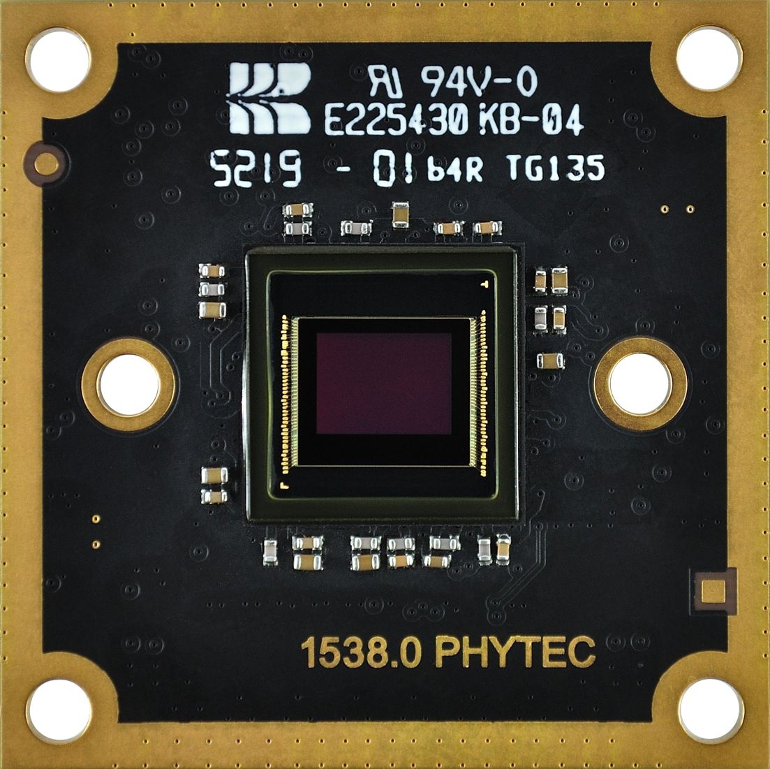
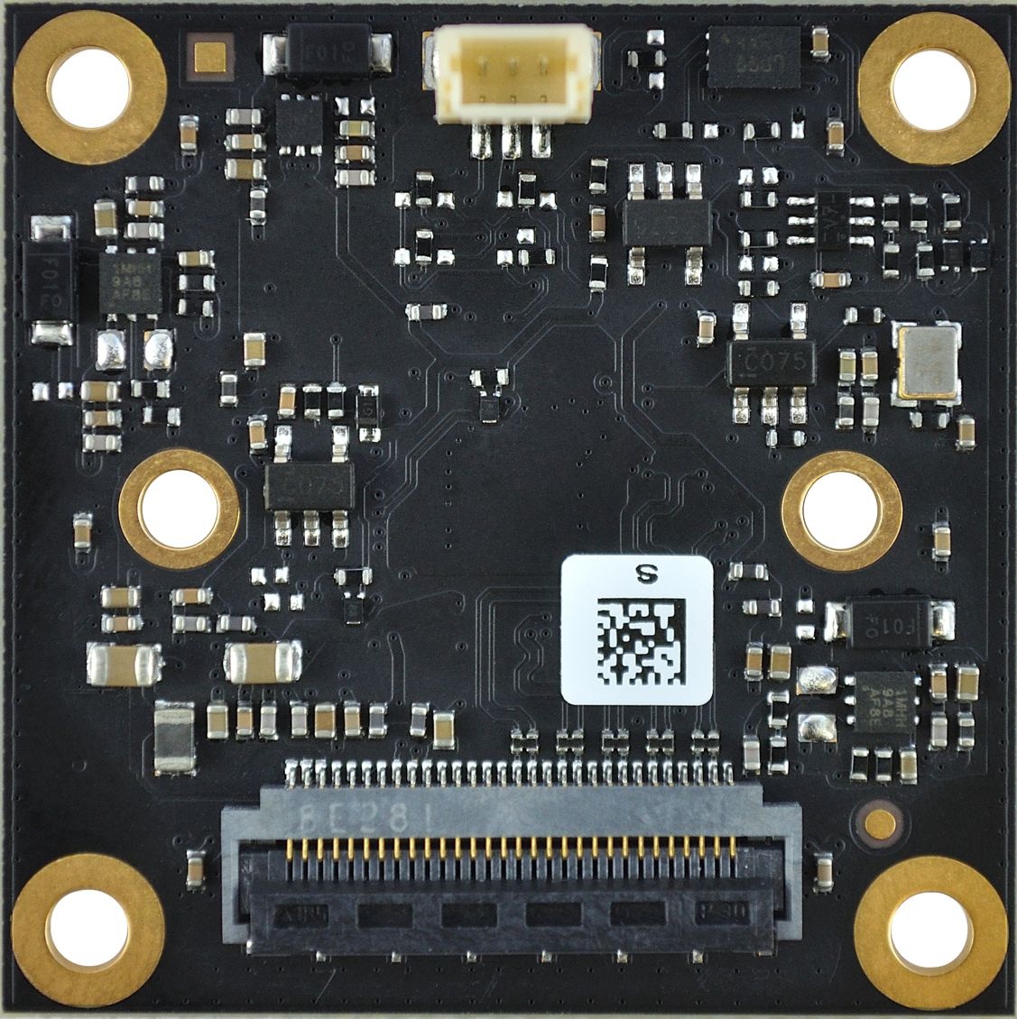
VM-017-xxx-M (phyCAM-M, PL1513.0) (Front/Back)
Specification
Function | VM-017-BW-M[1] | VM-017-COL-M[1] |
Camera Characteristics | ||
Resolution | 5,1 MPixel | 5,1 MPixel |
Resolution(H x V) | 2592 x 1944 Pixel | 2592 x 1944 Pixel |
Sensor size | 1/2.5" 5,7 mm x 4,28 mm | 1/2.5" 5,7 mm x 4,28 mm |
Pixel size | 2,2 µm x 2,2 µm | 2,2 µm x 2,2 µm |
Color/ monochrome | monochrome | color |
Sensor Technology | CMOS | CMOS |
Sensorchip | ON Semiconductor AR0521 | ON Semiconductor AR0521 |
Scan-System | progressive | progressive |
Shutter Type | rolling | rolling |
| ~60 fps (full Resolution) | ~60 fps (full Resolution) |
~125fps at 1080p | ~125 fps at 1080p | |
Sensitivity[2] | 36 ke-/lux×s | 18.8 ke−/lux×s |
SNRMAX[2] | 40 dB | 40 dB |
Dynamic Range[2] | 74.3 dB >96 dB Interleaved HDR | 74.3 dB >96 dB Interleaved HDR |
Exposure Time | programmable | programmable |
Amplification Analog / Digital | 1x … 16x / 1x … 8x | 1x … 16x / 1x … 8x per channel |
AEC /AGC | nein / nein | nein / nein |
Skipping | 2 / 3 / 4 | 2 / 3 / 4 |
Binning | yes | yes |
Chief Ray Angle | 9° | 9° |
External Trigger / Sync. | Trigger / Strobe | Trigger / Strobe |
ROI | yes | yes |
Mirror / Flip | yes | yes |
Image Processor | n/a | n/a |
LED Lighting | n/a | n/a |
Special Functions | ||
Electrical Interface | ||
Video Output Type | digital | digital |
Connection | phyCAM-M | phyCAM-M |
Data Format | MIPI CSI-2 (2-4 Data Lanes) | MIPI CSI-2 (2-4 Data Lanes) |
Interface Mode | Y8/Y10/Y12 | RGGB8/RGGB10/RGGB12 |
Camera Setting | I²C | I²C |
Supply Voltage | 3,3 V | 3,3 V |
Power Consumption (max) | 680 mW | 680 mW |
Power-up Standby (type) | 15 mW | 15 mW |
Mechanical Data | ||
Lens Mount | kein / M12 / C-CS | kein / M12 / C-CS |
Dimensions (mm) | 34 x 34 | 34 x 34 |
Mounting | 4 x M2.5 | 4 x M2.5 |
Weight (PCB) | 5 g | 5 g |
Connections | ||
phyCAM-M | Shielded FFC 30 pol. | Shielded FFC 30 pol. |
Trigger / Sync. | JST 3 pol. | JST 3 pol. |
VM-017-xxx-M (phyCAM-M) Specification
| 1. | n/a: not applicable. All data may be subject to technical changes |
| 2. | Specific specification of the sensor manufacturer. See datasheet of the sensor chip. |
Interface Characteristics
| Symbol | min | type | max | Unit |
Operating Voltage | VCAM | 3,0 | 3,3 | 3,6 | V |
Current Consumption | ICAM | - | 180 | - | mA |
MIPI CSI-2 DATA and CLK | see MIPI CSI-2 specification and the AR0521 Sensor Datasheet | ||||
I²C | see I2C specification for 3,3 V Fast-mode System | ||||
Input high voltage (Reset) | VIH_RST | 2,0 | 3,3 | 5,5 | V |
Input low voltage (Reset) | VIL_RST | -0,5 | 0 | 0,8 | V |
Input high voltage (I2C_ADR) | VIH_ADR | 1 | 3,3 | 3,6 | V |
Input low voltage (I2C_ADR) | VIL_ADR | - | - | 0,4 | V |
Input high voltage (CTRL2, CTRL4, TRIGGER_IN) | VIH | 2 | - | 5,5 | V |
Input low (CTRL2, CTRL4, TRIGGER_IN) | VIL | - | - | 0,8 | V |
Output high (CTRL1, CTRL3, STROBE_OUT) | VOH | Open-Drain (max. 5,5 Volt) | V | ||
Output low (CTRL1, CTRL3, STROBE_OUT) | VOL | - | - | 0,4 | V |
Output low (CTRL1, CTRL3, STROBE_OUT) | IOL | - | 10 | - | mA |
| TOP | -30 | - | Junction: <=85 Ambiente: < 65 | °C | |
Storage temperature[3] | TSTG | -30 | - | 85 | °C |
| MIPI CSI-2 Bus length on the Module | LMIPI | - | - | 25 | mm |
| MIPI CSI-2 Intra-Pair Skew on the Module | Ldiff-Intra | - | - | 50 | µm |
| MIPI CSI-2 Inter-Pair Skew on the Module | Ldiff-Inter | - | - | 500 | µm |
| Symbol | min | type | max | Unit |
Masterclock Frequency | fMCLK | - | 27 | - | MHz |
I²C Clock rate | fI2C | - | 100 | 400 | kHz |
| 3. | -25°C - +85°C with optional trigger/strobe socket. The junction temperature must not exceed 85°C. |
| 4. | The junction temperature can be read out. Depending on the operating state, the ambient temperature may fluctuate. |
Data Formats
monochrome (VM-017-BW-M):
- Y8 (8 Bit Grayscale resolution)
- Y10 (10 Bit Grayscale resolution)
- Y12 (12 Bit Grayscale resolution)
color (VM-017-COL-M):
- RGGB8 (8 Bit Bayer-Pattern)
- RGGB10 (10 Bit Bayer-Pattern)
- RGGB12 (12 Bit Bayer-Pattern)
I2C Addresses
|
| Configuration | Variant | |||||
I2C_ADDR | J19 | J20 | J21 | J22 | GPIO Camera Sensor | |||
| 0x6C | X | 2+3 | 1+2 | X | X | GPIO0_STROBE | all |
| X | 2+3 | X | 1+2 | X | GPIO1_SHUTTER | |||
| X | 2+3 | X | X | 1+2 | GPIO2_TRIGGER | |||
| GND | 2+4 | 1+2 | X | X | GPIO0_STROBE | |||
| GND | 2+4 | X | 1+2 | X | GPIO1_SHUTTER | |||
| GND | 2+4 | X | X | 1+2 | GPIO2_TRIGGER | |||
0x6E | X | 1+2 | 1+2 | X | X | GPIO0_STROBE | ||
| 1+2 | X | GPIO1_SHUTTER | ||||||
| X | 1+2 | X | X | 1+2 | GPIO2_TRIGGER | |||
| VCAM | 2+4 | 1+2 | X | X | GPIO0_STROBE | |||
| VCAM | 2+4 | X | 1+2 | X | GPIO1_SHUTTER | |||
| VCAM | 2+4 | X | X | 1+2 | GPIO2_TRIGGER | |||
VM-017 (phyCAM-M) I2C Addresses
The I²C addresses are specified hexadecimal in 8-bit representation. In Linux, it is possible to work with a 7-bit representation. In this case, the address value is to be shifted one digit to the right. The specification refers to the write address (bit 0 = 0). The read address is increased by 1 according to bit 1 = 1.
Additional I2C addresses can be configured within the camera sensor by using the software.
The address functionality must be enabled in the camera sensor and assigned to a GPIO before it can be used. For details, please refer to the sensor datasheet.
|
| Configuration |
| ||||
I2C_ADDR | J19 | J11 | J10 | J13 | |||
| 0xA0 | X | X | 1+2 | 1+2 | 2+3 |
|
0xA2 | X | X | 1+2 | 1+2 | 1+2 | ||
0xA4 | X | X | 1+2 | 2+3 | 2+3 | ||
0xA6 | X | X | 1+2 | 2+3 | 1+2 | ||
0xA8 | X | X | 2+3 | 1+2 | 2+3 | ||
0xAA | X | X | 2+3 | 1+2 | 1+2 | ||
0xAC | X | X | 2+3 | 2+3 | 2+3 | ||
0xAE | X | X | 2+3 | 2+3 | 1+2 | ||
0xAC | GND | 2+4 | 2+3 | 2+3 | 2+4 |
| |
0xAE | VCAM | 2+4 | 2+3 | 2+3 | 2+4 | ||
VM-017 (phyCAM-M) EEPROM I2C Addresses
The I²C addresses are specified hexadecimal in 8-bit representation. In Linux, it is possible to work with a 7-bit representation. In this case, the address value is to be shifted one digit to the right. The specification refers to the write address (bit 0 = 0). The read address is increased by 1 according to bit 1 = 1.
Feature Pins
Signal | Pin | Configurable Function | I/O | Configuration | GPIO Camera Sensor | Optional |
| CTRL1 | 11 | Strobe/Flash | O | J20: 2+4 | GPIO0_STROBE | |
CTRL2 | 12 | Trigger | I | J22: 2+4 | GPIO2_TRIGGER | |
| CTRL3 | 13 | Shutter | O | J21: 2+4 | GPIO1_SHUTTER | X |
CTRL4 | 14 | Trigger | I |
| GPIO0_STROBE | X |
CTRL4 | 14 | Trigger | I |
| GPIO1_SHUTTER | X |
CTRL4 | 14 | Trigger | I | J22: 2+3 | GPIO2_TRIGGER | X |
VM-017 (phyCAM-M) Feature Pins
Notes
Specify the internal configuration of the camera module to activate this function.
Functions can be mutually exclusive!
Furthermore, the camera sensor must be configured correctly to give the corresponding GPIO the correct functionality.
NOMT = not mounted = unassembled
Special configurations can be equipped by PHYTEC for series deliveries. Please contact our sales staff for further information.
The signals CTRL1 (Strobe Output) and CTRL3 (Shutter Output) are open-drain outputs. A pull-up resistor must be provided on the baseboard in each case.
Jumper Map

VM-017-xxx-M (phyCAM-M) Jumper Plan (PL1538.1)
Dimensioned Drawing
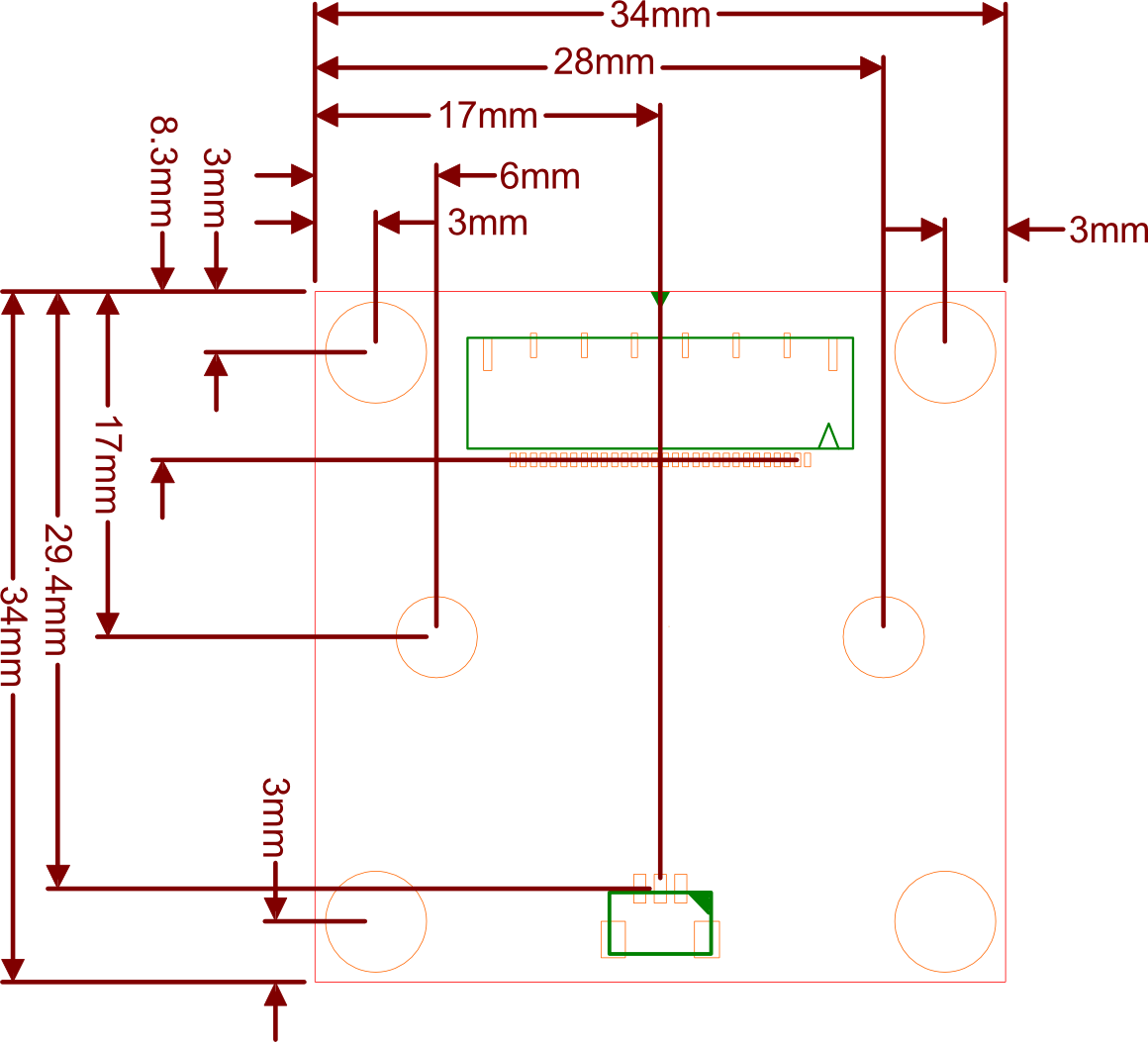
VM-017-xxx-M (phyCAM-M) Dimensional Drawing Connector Positions (backside)
Note
Current DXF and STEP data for your design are available on our website.
Special Functions
Trigger
The trigger input provides the following function:
- As an example, if the GPIO2 of the camera sensor connected to the trigger is configured as standby, a trigger function can be generated. A low level at the trigger input stops image acquisition in this case.
Details about triggering can be found in the datasheet of the camera sensor.
The trigger input is available at pin 1 of the expansion connector X2.
In addition, the trigger input is available at CTRL2 (pin 12) of the phyCAM-M connector.
Strobe
The strobe output provides the following functions:
- LED Flash: A high level is output during the exposure time of the image sensor. Here GPIO0 must be configured to flash.
- Xenon Flash: The strobe pulse is configurable. GPIO0 must be configured to flash.
Details about the strobe signal can be found in the datasheet of the camera sensor.
The strobe signal is available at pin 3 of the expansion connector X2. In addition, the strobe signal is available at CTRL1 (pin 11) of the phyCAM-M connector.
Note
The strobe signal is an open-drain output and requires a pull-up resistor on the application board.
Reset
See L-867Be.A0 phyCAM Digital Camera Modules Concept and Design-In Guide.
Revision History
Date | Version # | Changes in this manual |
01.03.2021 | Manual L-1021e.A0 | New Release |