


 Deutsch
  Englisch
  PHYTEC France
  PHYTEC USA
  PHYTEC India
  PHYTEC China
 Gesamtbetrag:
zzgl. Mwst.
Hardware Manual - phyCORE-i.MX 8M Plus FPSC (1617.3/1618.1)(L-1076e.A2)
Table of Contents
Information on this Manual
This hardware manual describes the PCL-078 System on Module, referred to as phyCORE®-i.MX 8M Plus FPSC. This manual also specifies the phyCORE-i.MX 8M Plus FPSC design and function. Precise specifications for the NXP® Semiconductor i.MX 8M Plus microcontrollers can be found in the i.MX 8M Plus Microcontroller Data Sheet/Reference Manual.
There will be several changes and additions to this manual. New versions will be released in the future with no notice. Please use this manual's latest version when working with your product.
Future Proof Solder Core
The PCL-078 System on Module is referred to as phyCORE®-i.MX 8M Plus FPSC is designed according to FPSC Gamma Feature Set Specifications (LAN-118e.A6).
Design Considerations
The schematics shown in this hardware manual are believed to be correct. However, correctness can not be guaranteed. The schematics have been pulled from PHYTEC's designs that have been built, tested, and are known to work. The schematics have been re-formatted to fit better in this hardware manual.
Many hardware examples and suggestions are given in the following pages. Designing the phyCORE System on Module onto a Carrier Board is generally straightforward. However, before committing to a particular active component selection when designing a carrier board, it is wise to check out the software driver support for those components. A particular device may be supported in, say, for example, Linux but not in Windows Embedded Compact 7. Your overall project may go smoother if you pick components that are already supported in your target OS. The premade selections for our reference designs, for example our Single Board Computers, are typically focused on using components that are well supported under Linux.
Specific details may need to be considered when designing a customer-specific carrier board. For design information on carrier board components, please check the Design Considerations in each component section of phyCORE-i.MX 8M Plus FPSC on the Libra Development Board. Be aware that not all components need to be considered when designing your own carrier board.
These manuals and more can be found in the download section of phyCORE-i.MX 8M Plus FPSC Product page.
Conversions, Abbreviations, and Acronyms
Tip
Due to part maintenance for our products (which are subject to continuous changes), we refrain from providing detailed, part-specific information within this manual. Please read the section Product Change Management and Information Regarding Parts Populated on the SOM / SBC within the Preface for more information.
Tip
The BSP that is delivered with the phyCORE-i.MX 8M Plus FPSC usually includes drivers and/or software for controlling all components, such as interfaces, memory, etc. Programming close to hardware at the register level is not necessary in most cases. For this reason, this manual does not contain detailed descriptions of the controller's registers or information relevant to software development. Please refer to the i.MX 8M Plus Reference Manual, if any information not found in this manual is needed to connect customer-designed applications.
Conventions
The conventions used in this manual are as follows:
- Signals that are preceded by an "n", "/", or “#”character (e.g.: nRD, /RD, or #RD), or that have a dash on top of the signal name (e.g.: RD) are designated as active low signals. That is, their active state is when they are driven low or are driving low.
- A "0" indicates a logic zero or low-level signal, while a "1" represents a logic one or high-level signal.
- The hex-numbers given for addresses of I2C devices always represent the 7 MSB of the address byte. The correct value of the LSB, which depends on the desired command (read (1), or write (0)), must be added to get the complete address byte. For example, if the given address in this manual is 0x41 =>, the complete address byte = 0x83 to read from the device and 0x82 to write to the device
- Tables that describe all settings show the default position in bold, blue text.
Types of Signals
Different types of signals are brought out at the phyCORE-Connector. The following table lists the abbreviations used to specify the type of signal.
| Signal Type | Description | Abbreviation |
|---|---|---|
| Power In | Supply voltage input | PWR_I |
| Power Out | Supply voltage output | PWR_O |
| Ref-Voltage | Reference voltage output | REF_O |
| Input | Digital input | I |
Output | Digital output | O |
| I/O | Bidirectional input/push-pull output | I/O |
| Input/OD-Output | Input / open-drain output requires an external pull-up | I/OD |
| OC-Bidir PU | Open collector input/output with pull-up | OC-BI-PU |
| OC-Output | Open-collector output without a pull-up requires an external pull-up | OC |
| OD-Bidir PU | Open-drain input/output with pull-up | OD-BI-PU |
| OD-Output | Open-drain output without a pull-up requires an external pull-up | OD |
| 5 V Input PD | 5 V tolerant input with pull-down | 5V-PD |
| USB IO | Differential line pairs 90 Ohm USB level bidirectional input/output | USB_I/O |
| ETHERNET Input | Differential line pairs 100 Ohm Ethernet level input | ETH_I |
| ETHERNET Output | Differential line pairs 100 Ohm Ethernet level output | ETH_O |
| ETHERNET IO | Differential line pairs 100 Ohm Ethernet level bidirectional input/output | ETH_I/O |
| PCIe Input | Differential line pairs 100 Ohm PCIe level input | PCIe_I |
PCIe Output | Differential line pairs 100 Ohm PCIe level output | PCIe_O |
PCIe IO | Differential line pairs 100 Ohm PCIe level input or output | PCIe_I/O |
| HDMI Input | Differential line pairs 100 Ohm HDMI level input | HDMI_I |
| HDMI Output | Differential line pairs 100 Ohm HDMI level output | HDMI_O |
MIPI CSI-2 Input | Differential line pairs 100 Ohm MIPI CSI‑2 level input | CSI2_I |
| MIPI DSI-2 Output | Differential line pairs 100 Ohm MIPI DSI-2 level output | DSI2_O |
| CAN FD IO | Differential line pairs 120 Ohm CAN FD level bidirectional input/output | CAN_I/O |
Signal Types
Abbreviations and Acronyms
Many acronyms and abbreviations are used throughout this manual. Use the following table to navigate unfamiliar terms used in this document.
| Abbreviation | Definition |
|---|---|
| BGA | Ball Grid Array |
BSP | Board Support Package (software delivered with the Development Kit, including an operating system (Windows or Linux) preinstalled on the module and development tools) |
CB | Carrier board; used in reference to the phyCORE development kit carrier board |
| DSC | Direct Soldering Contact |
EMI | Electromagnetic Interference |
FPSC | Future Proofed Soldering Core |
GPI | General-purpose input |
GPIO | General-purpose input and output |
GPO | General-purpose output |
IRAM | Internal RAM: the internal static RAM on the NXP® Semiconductor i.MX 8M Plus microcontroller |
J | Solder jumpers; these types of jumpers require solder equipment to remove and place |
JP | Solderless jumpers; these types of jumpers can be removed and placed by hand with no special tools |
| OEM | Original Equipment Manufacturers |
PCB | Printed circuit board |
| PCM | Product Change Management |
| PCN | Product Change Notification |
PMIC | Power management IC |
POR | Power On Reset |
RTC | Real-time clock |
| SBC | Single Board Computer |
SMT | Surface mount technology |
SOM | System on Module; used in reference to the PCM-070 /phyCORE®-i.MX 8M Plus module |
Sx | User button Sx (e.g. S1, S2, etc.) used in reference to the available user buttons, or DIP-Switches on the carrier board |
Sx_y | Switch y of DIP-Switch Sx; used in reference to the DIP-Switch on the carrier board |
| VM | Virtual Machine |
Abbreviations and Acronyms Used in this Manual
phyCORE-i.MX 8M Plus FPSC Introduction
The phyCORE‑i.MX 8M Plus FPSC belongs to PHYTEC’s phyCORE System on Module family. The phyCORE SoMs represent the continuous development of the PHYTEC System on Module technology. Like its mini-, micro-, and nanoMODUL predecessors, phyCORE boards integrate all core elements of a microcontroller system on a subminiature board and are designed in a manner that ensures their easy expansion and embedding in peripheral hardware developments.
Independent research indicates approximately 70 % of all Electromagnetic Interference (EMI) problems are caused by insufficient supply voltage grounding of electronic components in high-frequency environments. The phyCORE board design features an increased pin package, which allows for the dedication of approximately 20 % of all connector pins on the phyCORE boards to Ground. This improves EMI and EMC characteristics and makes it easier to design complex applications meeting EMI and EMC guidelines using phyCORE boards, even in high-noise environments.
phyCORE boards achieve their small size through modern SMT and multi-layer design. Due to the complexity of our modules, 0201-packaged SMT components and laser-drilled microvias are used on the boards, providing phyCORE users with access to this cutting-edge miniaturization technology for integration into their own design.
The phyCORE‑i.MX 8M Plus FPSC is a subminiature (40 mm x 37 mm) insert-ready System on Module populated with the NXP® Semiconductor i.MX 8M Plus microcontroller. Its universal design enables it to be inserted into a wide range of embedded applications. All controller signals and ports extend from the controller to surface mount technology (FPSC FTGA 1.27 mm grid) connectors, aligning four sides of the board, allowing it to be soldered into any target application like a "big chip".
The descriptions in this manual are based on the NXP® Semiconductor i.MX 8M Plus. Descriptions of compatible microcontroller derivative functions are not included, as such functions are not relevant for the basic functioning of the phyCORE‑i.MX 8M Plus FPSC.
phyCORE-i.MX 8M Plus FPSC Features
The phyCORE‑i.MX 8M Plus FPSC offers the following features:
- Insert-ready, sub-miniature (40 mm x 37 mm) System on Module (SOM) subassembly in low EMI design, achieved through advanced SMD technology
- Mounted using FTGA Direct Solder Connector (FPSC FTGA)
- Populated with the NXP® Semiconductor i.MX 8M Plus microcontroller (BGA548 packaging)
- Up to 4 ARM-A53 cores (clock frequency up to 1.8 GHz)
- Machine Learning Neuronal Processing Unit (NPU) with 2.3 TOPS
- 1x Cortex M7 core (800 MHz). All Cortex M7 dedicated interfaces are explicitly made available on the SoM connector.
- Tensilica Hifi4 Audio DSP (800 MHz)
- 3D GPU GC7000UL and 2D GPU GC520L
- Neural Network Accelerator (up to 2.3TOPS)
- on-board Image Signal Processor (up to 12MP resolution/ up to 375MP/s)
- Boot from different memory devices (eMMC Flash standard)
- Single supply voltage of +5.0 V with on-board power management
- Selectable IO voltage between 1.8 V and 3.3 V (1.8 V is the default according to FPSC Specification)
- All controller-required supplies are generated onboard using sophisticated onboard Power Management
- Improved interference safety achieved through multi-layer PCB technology and dedicated ground pins
up to 8 GB[1] LPDDR4 RAM
- up to 64 GB[1] on-board eMMC in the commercial temperature range (up to 32 GB for I-Temp)
- 4kB[1]I2C User-EEPROM and 4kB I2C Factory-EEPROM
- 2x USB 3.0/2.0 Dual-Role interfaces with PHY
2x 1Gbit Ethernet interfaces with TSN support (either one of them with Ethernet transceiver on the phyCORE-i.MX 8 M Plus FPSC enabling a direct connection to an existing Ethernet network; the second as RGMII Signals at logic-level at the signal pins instead)
- 5x I2C interfaces
- 2x SPI interfaces
- 1x PCIe interface
- 3x UART interfaces
- 2x CAN-FD interfaces
- 4x PWM outputs
- 1x MIPI DSI-2 interface
- 1x HDMI interface
- 2x MIPI CSI-2 camera interfaces
- 1x LVDS Tx interface 2 channels x4
- 1x 4-bit SD-Card interface
- 1x 4-bit SDIO interface
- 1x SAI audio interfaces
- Extreme Low Power RTC Module
- 4x temperature sensors to monitor the board's temperature profile
- All processor interfaces available at the SoM Connector
- Available for different temperature grades (see Product Temperature Grades)
phyCORE-i.MX 8M Plus FPSC Block Diagram
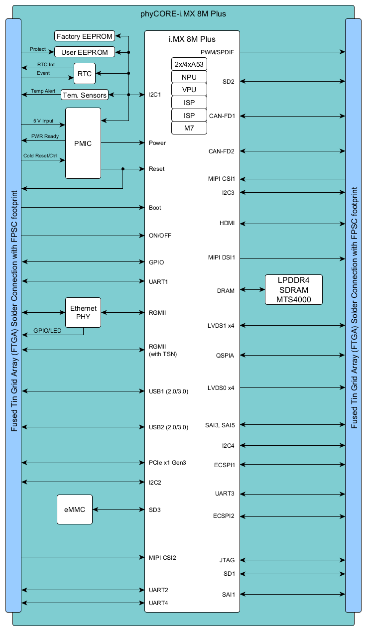
phyCORE-i.MX 8M Plus FPSC Block Diagram
phyCORE-i.MX 8M Plus FPSC Component Placement
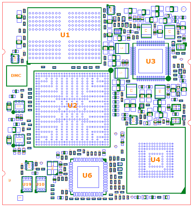
phyCORE-i.MX 8M Plus FPSC Component Placement (1617.3 Top View)
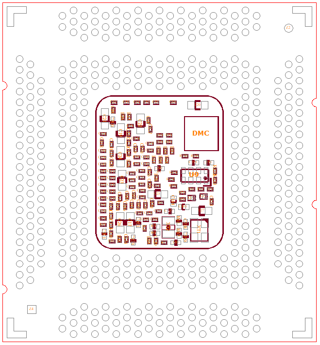
phyCORE-i.MX 8M Plus FPSC Component Placement (1617.3 Bottom View)
phyCORE-i.MX 8M Plus FPSC Minimum Operating Requirements
Warning
We recommend connecting all available VIN (+5.0 V) input contacts to the power supply system on a custom carrier board housing the phyCORE-i.MX 8M Plus FPSC. In addition, proper implementation of the phyCORE-i.MX 8M Plus FPSC module into a target application also requires connecting all GND contacts.
Refer to Power for more information.
Before the phyCORE-i.MX 8M Plus FPSC can be used, please make sure the host system meets the minimum operating requirements. These include:
- The stable and clean input power supply of 5.0 V with low ESR bulk capacitors (e.g. 2x 47µ/16V MLCC) paired with some HF blocking capacitors (e.g. 100nF/16V MLCC) connected to the input pins as near as possible (phyCORE-i.MX 8M Plus FPSC Power Consumption). It is recommended to monitor the supplied input voltage against minimum voltage level 4.75 V and drive X_POR_B_VIO low if the input voltage is below.
- Appropriate configuration of the I/O voltage (1.8 V default or 3.3 V) configured by signal X_VIO_Ctrl (External Logic IO Supply Voltage)
- Supply voltage for externally connected peripherals should be controlled by signal X_nPWR_READY to avoid reverse currents (External Logic IO Supply Voltage)
- If external peripherals need a longer reset delay, hold reset signal X_POR_B_VIO as long low as needed (Reset)
- Desired boot configuration - default configuration is "Boot from on-board eMMC" (System Boot Configuration)
- To back up the on-board I2C-RTC, connect a buffer voltage source to input pin X_RTC_VBACKUP (Backup Power (X_RTC_VBACKUP / VIN_SNVS_1V8), RTC)
Pin Description
Warning
Module connections must not exceed their expressed maximum voltage or current. Maximum signal input values are indicated in the corresponding controller manuals/datasheets. As damage from improper connections varies according to use and application, the user must take appropriate safety measures to ensure that the module connections are protected from overloading through connected peripherals.
All controller signals extend to FPSC footprint. These contacts line four sides of the module (referred to as FPSC footprint). This enables phyCORE-i.MX 8 Plus FPSC to be placed into any target application like a "big chip".
PHYTEC provides a complete pinout table for the phyCORE-i.MX 8M Plus FPSC Footprint (X1). This table contains a complete signal path for the phyCORE‑i.MX 8M Plus FPSC and the carrier board PCM-937-L, including signal names, pin muxing paths, and descriptions specific to each pin. It also provides the appropriate voltage domain, signal type (ST), and a functional grouping of the signals. The signal type also includes information about the signal direction. A table describing the signal types can be found with the phyCORE-i.MX 8M Plus FPSC Pinout Table.
Warning
- The NXP® Semiconductor i.MX 8M Plus is a multi-voltage operated microcontroller and, as such, special attention should be paid to the interface voltage levels to avoid unintentional damage to the microcontroller and other on-board components. Please refer to the NXP Semiconductor i.MX 8M Plus Reference Manual for details on the functions and features of controller signals and port pins.
- As some of the signals that are brought out on the phyCORE-Footprint are used to configure the boot mode for specific boot options, please make sure that these signals are not driven by any device on the baseboard during reset. The signals that may affect the boot configuration are shown inphyCORE-Connector Boot Configuration Pins.
- It is necessary to avoid voltages at the IO pins of the phyCORE-i.MX 8M Plus FPSC which are sourced from the supply voltage of peripheral devices attached to the SOM during power-up or power-down. These voltages can cause a current flow into the controller, especially if peripheral devices attached to the interfaces of the i.MX 8M Plus are supposed to be powered while the phyCORE‑i.MX 8M Plus FPSC is in suspend mode or turned off. To avoid this, bus switches are either supplied by VDD_1V8 on the phyCORE side or have their output enabled to the SOM controlled by the X_nPWR_READY signal (see Supply Voltage for External Logic) must be used.
Pin Muxing Warning
If pin settings are changed from the PHYTEC standard configuration, make sure that the setting of the pull resistors are adjusted accordingly. Never rely on the SoC-internal pull resistor.
Jumpers
The phyCORE-i.MX 8M Plus FPSC (PCL-078) is jumperless. There are, however, a few jumpers on the Baseboard PCM-937-L. Information on these jumpers can be found inJumpers.
Warning
Due to the small footprint of the solder jumpers (J), PHYTEC does not recommend manual jumper modifications. This may also render the warranty invalid. Contact our sales team if you need jumper configurations different from the default configuration.
Power
The phyCORE‑i.MX 8M Plus FPSC operates off of a single power supply voltage. The following section discusses the primary power pins on the phyCORE i.MX 8M Plus Connector X1 in detail.
Primary System Power (VIN)
The phyCORE‑i.MX 8M Plus FPSC is powered by a primary voltage supply with a nominal value of +5.0 V. On-board switching regulators generate the voltage supplies required by the i.MX 8M Plus MCU and on-board components from the primary 5.0 V supplied to the SOM.
For proper operation, the phyCORE‑i.MX 8M Plus FPSC must be supplied with a voltage source of 4.75 ... 5.25 V with a maximum power consumption of a 2.5 A load at the VIN pins on the phyCORE.
Connect all +5.0 V VIN input pins to your power supply and all GND contacts of the module.
FPSC Contact | FPSC Signal | SOM Signal Name | Signal Type | Description |
|---|---|---|---|---|
| L24, M25, N24, L22, N22, M21, N20, P21 | VCC_IN | VIN | PWR_I | 5 V ± 5% Power supply input of the modul. |
| M23, P23, T23, V23, Y23, AB23, AD23, AF23, AH23, AH27, AH31, AH35, AH39, AH43, AH47, AH51, AH55, AH59, AF59, AD59, AB59, Y59, V59, T59, P59, M59, M55, M51, M47, M43, M39, M35, M31, M27, M13, P13, T13, V13, Y13, AB13, AD13, AF13, AH13, AM23, AM27, AM31, AM35, AM39, AM43, AM47, AM51, AM55, AM59, AH69, AF69, AD69, AB69, Y69, V69, T69, P69, M69, H59, H55, H51, H47, H43, H39, H35, H31, H27, H23 | 0V GND | GND | GND | Power and signal ground reference. |
| 1, 2, 3, 4 (Corner GND) | 0V GND | GND | GND | Mechanical fixing, power, and signal ground reference. |
Primary System Power (VIN) Pinout
Please refer to section Pin Description for information on additional GND Pins located at the phyCORE i.MX 8M Plus FPSC Connector X1.
For information on various power consumption scenarios that PHYTEC has run, go to phyCORE-i.MX 8M Plus FPSC Power Consumption.
Warning
As a general design rule, PHYTEC recommends connecting all GND pins to neighboring signals that are being used in the application circuitry. For maximum EMI performance, all GND pins should be connected to a solid ground plane. Additionally, take care of a solid, low impedance connection of the power supply line to avoid voltage drop. It is recommended to place a couple of bulk capacitors as near as possible to the phyCORE's system power input (VIN) to compensate for the trace inductance.
Power Management IC (PMIC) (U3)
The phyCORE-i.MX 8M Plus FPSC provides an on-board Power Management IC (PMIC) at position U3 to generate different voltages required by the microcontroller and the on-board components. The PMIC supports many functions like different power management functionalities like dynamic voltage control, different low power modes, and regulator supervision. It is connected to the i.MX 8M Plus via the on-board I2C bus (I2C1). The I2C address of the PMIC is 0x25.
Power Domains
External voltages to supply the board:
- VIN 5.0 V main supply voltage (4.75 .. 5.5 V / max. 2.5 A)
- optional: VIN_SNVS_1V8 low power supply voltage input (1.8 V ±5% / 10mA; if left open, it is provided on-board if VIN is present)
- X_RTC_VBACKUP (e.g. 3.3 V) backup supply voltage for the on-board I2C-Bus RTC U9 (RV-3028-C7)
External Logic IO Supply Voltage
The voltage level (VDD_IO) of the phyCORE’s logic interface circuitry is VDD_1V8 (1.8 V) or VDD_3V3 (3.3 V), which is determined by the configuration input signal X_VIO_Ctrl (X1-Y25). Connect X_VIO_Ctrl to the module input supply voltage VIN (5V) to configure VDD_IO=3.3 V interface voltage level or connect it to GND or leave it open (has onboard pull-down) to select VDD_IO=1.8 V interface voltage level.
To follow the power-up and power-down sequencing mandatory for the i.MX 8M Plus, external devices connected to the phyCORE interface circuitry have to be supplied by an external power supply, which is controlled by the output signal X_nPWR_READY (OD driver) which is brought out at pin X1-U22. X_nPWR_READY should control the external supply voltage which is used to supply the external interface circuitry connected to the phyCORE's interfaces. X_nPWR_READY switches from High-Z to GND to start the external voltage supply or to switch over a power switch. If the on-board interface voltage (VDD_IO) switches off, X_nPWR_READY is released to high impedance. To raise the signal, an external pull-up resistor (e.g, 4k7) is needed. It can be connected to voltage levels up to 10V (used Transistor DMN1260UFA has abs. max. 12 V), depending on the external power supply control signal requirement. The use of X_nPWR_READY ensures that external components are only supplied when the supply voltages of the i.MX 8M Plus is stable and avoids undefined return currents while the system is powered down.
SOM Connector Pin / Libra Development Board Carrier Board Connector Pin | FPSC Signal | SOM Signal Name | SOM Voltage Domain | Signal Level | Signal Type | Description |
|---|---|---|---|---|---|---|
| Y25 | Proprietary | X_VIO_Ctrl | - | 5 V | I | VDD_IO voltage level selection. Leave the input open or connect it to GND for VDD_IO = 1.8 V (default) or connect it to VIN (5V) to define VDD_IO = 3.3 V. |
| U22 | nPWRREADY_OUT | X_nPWR_READY | - | abs. max 12 V | OD | Needs an external PU-Resistor (abs. max. 12 V). Use it to control the power sequencing of your baseboard. |
External Logic IO Supply Voltage Pinout
Warning
PHYTEC recommends monitoring the externally generated power supply voltages with a voltage supervisor. The supervisor should hold X_POR_B_VIO (X1-R22) low, as long as the externally generated voltages are not properly maintained. To drive X_POR_B_VIO to GND, use an open-drain driver (OD) or N-channel FET (e.g. DMN1260UFA). X_POR_B_VIO has an on-board pull-up resistor to VDD_IO.
Backup Power (X_RTC_VBACKUP / VIN_SNVS_1V8)
To back up the on-board I2C-Bus RTC U9 (RV-3028-C7), an external voltage source must be added at Pin X1-AA22 (X_RTC_VBACKUP). The RTC has an extremely low backup current consumption of only 40nA (@3 V). It is also possible to supply the internal RTC and some critical registers of the i.MX 8M Plus' low power domain (NVCC_SNVS_1V8). NVCC_SNVS_1V8 can be supplied over Pin X1-J24 if VIN is not present.
SOM Connector Pin / Libra Development Board Carrier Board Connector Pin | FPSC Signal | SOM Signal Name | SOM Voltage Domain | Signal Level | Signal Type | Description |
|---|---|---|---|---|---|---|
| AA22 | VCC_RTC | X_RTC_VBACKUP | - | nom. 3.3 V (max. range 1.1 V to 5.5 V) | PWR_I | Connect a gold cap or a battery here. If a battery is used, make sure that the RTC trickle charger is deactivated! |
| J24 | Proprietary | VIN_SNVS_1V8 | - | 1.8 V ± 5% | PWR_I | Optional backup supply input for NVCC_SNVS_1V8. If not required, leave it open. |
Backup Power (X_RTC_VBACKUP / VIN_SNVS_1V8) Pinout
Manual Power Switch (X_OnOff)
The signal X_OnOff (Pin X1-R20) is used to manually switch the power of the SOM. X_OnOff signal can be left unconnected if not used. It has a weak on-board pull-up resistor against NVCC_SNVS_1V8 and is held high as long as VIN is present or external backup voltage VIN_SNVS_1V8 is supplied. To drive the signal to GND, use an open collector driver or push button. For more information about ON/OFF refer to the NXP Semiconductor i.MX 8M Plus Reference Manual.
SOM Connector Pin / Libra Development Board Carrier Board Connector Pin | FPSC Signal | SOM Signal Name | SOM Voltage Domain | Signal Level | Signal Type | Description |
|---|---|---|---|---|---|---|
| R20 | ON/OFF | X_OnOff (G22) | NVCC_SNVS_1V8 | 1.8 V | I | Wake up and power off the Processor. Intended to connect a push-button or an open-collector driver. |
Backup Power (X_RTC_VBACKUP / VIN_SNVS_1V8) Pinout
Reset
The X_nRESET_IN signal (Pin X1-Y21) on the phyCORE-Connector is designated as a "cold reset" input. Driving X_nRESET_IN to low (has 10k pull-up to VIN) will restart the system, performing a complete power recycle. Holding X_nRESET_IN low will force the system reset and hold it in the reset state. This input can be used for a mechanical reset switch button. X_POR_B_VIO Signal (Pin X1-R22) is the global system reset output. This can be used as a startup as described in the section Power Management IC.
SOM Connector Pin / Libra Development Board Carrier Board Connector Pin | FPSC Signal | SOM Signal Name | SOM Voltage Domain | Signal Level [2] | Signal Type | Description |
|---|---|---|---|---|---|---|
| Y21 | nRESET_IN | X_nRESET_IN | VIN | 5.0 V (module input supply voltage) | OD_IN | X_nRESET_IN acts as a cold reset input. Driving X_nRESET_IN to low (has 10k pull-up to VIN) will restart the system, performing a complete power recycle triggert from the falling edge of the signal. Holding X_nRESET_IN low will force the system reset and hold it in the reset state. This input can be used for a mechanical reset switch button. |
| R22 | nRESET_OUT | X_POR_B_VIO (via level shift to J29) | VDD_IO | 1.8 V / 3.3 V | OD | This pin is internally connected to the processor and the PMIC. Connect it to the reset input of your baseboard peripherals. |
| 2. | VDD_IO Signal Level is default 1.8 V according to FPSC Specification. |
Reset Pinout
System Boot Configuration
Most features of the i.MX 8 Plus microcontroller are configured and/or programmed during the initialization routine. Other features, which impact program execution, must be configured before initialization via pin termination.
The system start-up configuration includes:
- Boot mode selection
- Boot device selection
- Boot device configuration
The internal ROM code is the first code executed during the initialization process of the i.MX 8M Plus after POR. The ROM code detects the boot mode by using the boot mode pins (BOOT_MODE[3:0]), while the boot device is selected and configured by determining the state of the eFUSEs and/or the corresponding GPIO input pins (X_BOOT_MODE[3:0]).
Boot Mode Selection
The boot mode of the i.MX 8M Plus microcontroller is determined by the configuration of four boot mode inputs BOOT_MODE[3:0] during the reset cycle of the operational system. These inputs are brought out at the phyCORE processor pins X_BOOT_MODE[3:0] (X1-P25, X1-R24, X1-T25, X1-U24). phyCORE-i.MX 8M Plus FPSC Boot Modes shows the possible settings of pins X_BOOT_MODE[3:0] and the resulting boot configuration of the i.MX 8M Plus.
| Boot Mode | X_BOOT_MODE3 | X_BOOT_MODE2 | X_BOOT_MODE1 | X_BOOT_MODE0 | Boot Source |
|---|---|---|---|---|---|
| 0 | 0 | 0 | 0 | 0 | Boot from internal fuses |
| 0 | 0 | 0 | 0 | 1 | USB Serial Downloader |
| 2 | 0 | 0 | 1 | 0 | Boot from onboard eMMC (default) |
| 3 | 0 | 0 | 1 | 1 | Boot from ext. SD-Card on SD2 |
| 6 | 0 | 1 | 1 | 0 | Boot from onboard QSPI Flash |
| 15 | 1 | 1 | 1 | 1 | JTAG mode |
phyCORE-i.MX 8M Plus FPSC Boot Modes
The X_BOOT_MODE[3,2,0] lines have 100 kΩ pull-down resistors populated (and unpopulated pull-up resistors) while X_BOOT_MODE[1] has a 4,7 kΩ pull-up resistor on the module in parallel to the internal pull-down resistors of the i.MX8 M Plus. Leaving the four pins unconnected sets the controller to boot mode 1, boot from the onboard eMMC U4 memory device. The boot configuration settings can be changed by changing the populated resistors configuration on the module or by connecting configuration resistors (e.g. 4,7 kΩ pull-up) to the X_BOOT_MODE configuration signals. The pull-up resistors must be supplied by the right VDD_IO voltage level of 1.8 V (default according to FPSC Specification) or 3.3 V, depending on the VDD_IO configuration (see section External Logic IO Supply Voltage).
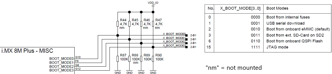
phyCORE-i.MX 8M Plus onboard Boot Configuration Schematic
The BOOT_MODE is initialized by sampling the BOOT_MODE inputs on the rising edge of the POR_B. After these inputs are sampled, their subsequent state does not affect the contents of the BOOT_MODE internal register, and the pins can be used for GPIO operation.
SOM Connector Pin / Libra Development Board Carrier Board Connector Pin | FPSC Signal Must-Have | SOM Signal Name | SOM Voltage Domain | Signal Level [2] | Signal Type | Description |
|---|---|---|---|---|---|---|
| P25 | BOOT_MODE1 | X_BOOT_MODE0 (G10) | VDD_IO | 1.8 V / 3.3 V | I/O | Boot configuration pin 0 during reset has on-board 100k pull-down resistor (SMD 0201) |
| R24 | BOOT_MODE2 | X_BOOT_MODE1 (F8) | VDD_IO | 1.8 V / 3.3 V | I/O | Boot configuration pin 1 during reset has on-board 4,7 k pull-down resistor (SMD 0201) |
| T25 | BOOT_MODE3 | X_BOOT_MODE2 (G8) | VDD_IO | 1.8 V / 3.3 V | I/O | Boot configuration pin 2 during reset has onboard 100k pull-down resistor (SMD 0201) |
| U24 | BOOT_MODE4 | X_BOOT_MODE3 (G12) | VDD_IO | 1.8 V / 3.3 V | I/O | Boot configuration pin 3 during reset has onboard 100k pull-down resistor (SMD 0201) |
| 2. | VDD_IO Signal Level is default 1.8 V according to FPSC Specification. |
phyCORE-i.MX 8M Plus FPSC Boot Configuration Pins
System Memory
The phyCORE‑i.MX 8M Plus FPSC provides three types of on-board memory:
| Basic-Version | Kit-Version | Exclusive-Version | Maximum Available | |
|---|---|---|---|---|
| One bank LPDDR4 RAM | 1 GByte | 2 GByte | 4 GByte | 8 GByte |
| eMMC | 4 GByte | 8 GByte | 32 GByte | 64 GByte |
| I2C User EEPROM | 4 kB | 4 kB | 4 kB | 32 kB |
I2C Factory EEPROM [3] | 4 kB | 4 kB | 4 kB | 32 kB |
phyCORE‑i.MX 8M Plus FPSC Onboard Memory Types
| 3. | Factory EEPROM should not be used by the application. It contains module-specific information to identify the module during factory handling and testing. |
LPDDR4-RAM (U1)
The RAM memory interface of the phyCORE‑i.MX 8M Plus FPSC supports one 32-bit LPDDR4-RAM chip (U1). The LPDDR4 memory is accessible starting at addresses 0x4000 0000 and 1 0000 0000.
Typically, the LPDDR4-RAM initialization is performed by a boot loader or operating system following a power-on reset and must not be changed at a later point by any application code. When writing custom code independent of an operating system or boot loader, the RAM must be initialized by accessing the appropriate RAM configuration registers on the i.MX 8M Plus controller. Refer to the NXP Semiconductor i.MX 8M Plus Reference Manual to access and configure these registers.
eMMC Flash Memory (U4)
The main flash memory of the phyCORE‑i.MX 8M Plus FPSC is eMMC and is populated at U4. The eMMC Flash memory is connected to the SD3 interface of the i.MX 8M Plus.
For more information about the eMMC Flash interface, please refer to the NXP Semiconductor i.MX 8M Plus Reference Manual.
I2C Factory EEPROM (U10)
The phyCORE‑i.MX 8M Plus FPSC is populated with a non-volatile 4 kB I2C EEPROM at U10. This memory is used to store configuration data and should not be used for different purposes. This device is accessed through I2C port 1 on the i.MX 8M Plus. The control registers for I2C port 1 are mapped between addresses 0x30A2 0000 and 0x30A3 0000. Please see the NXP Semiconductor i.MX 8M Plus Reference Manual for detailed information on the registers.
The three lower address bits are fixed to 0x1, which means that the EEPROM can be accessed at I2C address 0x51. The EEPROM has a second address on 0x59, which is called the Identification Page.
The device is write-protected by default. Write protection can be deactivated by driving the signal X_EEPROM1_WC (X1-DE21) to GND. The signal has a 10k pull-up resistor to VDD_IO (default 1.8 V).
I2C User EEPROM (U18)
The phyCORE‑i.MX 8M Plus FPSC is populated with a non-volatile 4 kB I2C EEPROM at U18. This memory is free for use. This device is accessed through I2C port 1 on the i.MX 8M Plus. The control registers for I2C port 1 are mapped between addresses 0x30A2 0000 and 0x30A3 0000. Please see the NXP Semiconductor i.MX 8M Plus Reference Manual for detailed information on the registers.
The three lower address bits are fixed to 0x1, which means that the EEPROM can be accessed at I2C address 0x50. The EEPROM has a second address on 0x58, which is called the Identification Page.
The device is not write-protected by default. Write protection can be established by driving the signal X_EEPROM2_WC (X1-DF20) to VDD_IO (default 1.8 V). The signal has a 10k pull-down resistor.
Serial Interfaces
The phyCORE‑i.MX 8M Plus FPSC provides numerous dedicated serial interfaces, some of which are equipped with a transceiver to enable direct connection to external devices:
- 1x 4-bit SDIO interface (SD2) with controlled IO voltage
- 1x 4-bit SDIO interface (SD1)
- 1x QSPI interface
- 3x high-speed UARTs
- 2x CAN-FD interfaces
- 2x USB 3.0/2.0 Dual-Role interfaces with PHY
- 2x 1Gbit Ethernet interfaces with TSN support (ENET1 with Ethernet transceiver on the phyCORE-i.MX 8 M Plus FPSC enabling a direct connection to an existing Ethernet network; ENET0 as RGMII Signals at logic-level at the signal pins instead)
- 5x I2C interfaces
- 2x Serial Peripheral Interfaces (SPI)
- 1x SAI audio interface
- 1x PCI Express with x1 interface
- 2x MIPI CSI-2 camera interfaces
- 1x MIPI DSI-2 display interface
Details for each of these serial interfaces and any applicable jumper configurations are below.
SDIO Interface
The SDIO interface can be used to connect external SD cards, eMMC, or any other device requiring an SDIO interface (i.e. WiFI, I/O expansion, etc.) The phyCORE bus features one SDIO interface. On the phyCORE‑i.MX 8M Plus FPSC, the interface signals extend from the first and second Ultra Secured Digital (SD1 and SD2) Host controller to the phyCORE-Connector.
The tables below show the location of the different interface signals on the phyCORE-Connector. The MMC/SD/SDIO Host Controller is fully compatible with the SD Memory Card Specification 3.0. The interface supports SD cards with 1.8 V and 3.3 V I/O signals.
SDIO SD2 (4-bit)
SDIO SD2 is a 4-bit wide interface with controlled I/O voltage to support high-speed modes that require 1.8 V I/O voltage. During runtime, the I/O voltage can be switched from 3.3 V (default) to 1.8 V by the processor via GPIO signal X_PMIC_SD_VSEL/GPIO1_IO04 which controls the PMIC integrated voltage regulator. X_VDDSW_SD2 will be used exclusively to supply an external SD or MicroSD memory card. X_VDDSW_SD2 is monitored by the PMIC load switch circuit for overcurrent and short circuits. For more details, please refer to the PMIC data sheet provided by NXP.
SOM Connector Pin / Libra Development Board Carrier Board Connector Pin | FPSC Signal Must-Have | SOM Signal Name | SOM Voltage Domain | Signal Level | Signal Type | Muxing / Description |
|---|---|---|---|---|---|---|
Y57 | SDCARD_VCC_OUT | X_VDDSW_SD2 | VDD_3V3 | 3.3 V | PWR_O | Controlled SD Card Supply Voltage |
| V57 | SDCARD_nCD | X_SD2_CD_B (AD48) | NVCC_SD2 | 1.8 V / 3.3 V | I | SD2 Card Detect |
V67 | SDCARD_WP | X_SD2_WP (AC26) | NVCC_SD2 | 1.8 V / 3.3 V | OD | SD2 Write Protect |
| W58 | SDCARD_CMD | X_SD2_CMD (AB28) | NVCC_SD2 | 1.8 V / 3.3 V | I/O | SD2 Command |
| W60 | SDCARD_CLK | X_SD2_CLK (AB29) | NVCC_SD2 | 1.8 V / 3.3 V | O | SD2 Clock |
| W62 | SDCARD_DATA0 | X_SD2_DATA0 (AC28) | NVCC_SD2 | 1.8 V / 3.3 V | I/O | SD2 Data 0 |
| Y61 | SDCARD_DATA1 | X_SD2_DATA1 (AC29) | NVCC_SD2 | 1.8 V / 3.3 V | I/O | SD2 Data 1 |
| U60 | SDCARD_DATA2 | X_SD2_DATA2 (AA26) | NVCC_SD2 | 1.8 V / 3.3 V | I/O | SD2 Data 2 |
| V61 | SDCARD_DATA3 | X_SD2_DATA3 (AA25) | NVCC_SD2 | 1.8 V / 3.3 V | I/O | SD2 Data 3 |
SDIO Interface Pinout of SD2
SDIO SD1 (4-bit)
SDIO SD1 is a 4-bit wide interface. The I/O voltage is determined by VDD_IO, which is statically configured for the system to 1.8 V or 3.3 V (refer to External Logic IO Supply Voltage).
SOM Connector Pin / Libra Development Board Carrier Board Connector Pin | FPSC Signal Must-Have | SOM Signal Name | SOM Voltage Domain | Signal Level [2] | Signal Type | Muxing / Description |
|---|---|---|---|---|---|---|
| G56 | SDIO_CMD | X_SD1_CMD (W29) | VDD_IO | 1.8 V / 3.3 V | I/O | SD1 Command |
| H57 | SDIO_CLK | X_SD1_CLK (W28) | VDD_IO | 1.8 V / 3.3 V | O | SD1 Clock |
| G62 | SDIO_DATA0 | X_SD1_DATA0 (Y29) | VDD_IO | 1.8 V / 3.3 V | I/O | SD1 Data 0 |
| H61 | SDIO_DATA1 | X_SD1_DATA1 (Y28) | VDD_IO | 1.8 V / 3.3 V | I/O | SD1 Data 1 |
| G60 | SDIO_DATA2 | X_SD1_DATA2 (V29) | VDD_IO | 1.8 V / 3.3 V | I/O | SD1 Data 2 |
| G58 | SDIO_DATA3 | X_SD1_DATA3 (V28) | VDD_IO | 1.8 V / 3.3 V | I/O | SD1 Data 3 |
| G54 | SDIO_WP | X_GPIO1_IO07 (F6) | VDD_IO | 1.8 V / 3.3 V | OD | GPIO1_IO07 used for SD1 Write Protect |
| J58 | SDIO_CD | X_GPIO1_IO06 (A3) | VDD_IO | 1.8 V / 3.3 V | OD | GPIO1_IO06 used for SD1 Card Detect |
| J56 | SDIO_VIO_OUT | VDD_IO | VDD_IO | 1.8 V / 3.3 V | PWR_O | Voltage output (max. 20mA) to supply VDD_IO of the connected device |
| 2. | VDD_IO Signal Level is default 1.8 V according to FPSC Specification. |
SDIO Interface Pinout of SD1
Universal Asynchronous Interfaces (UARTs)
The phyCORE‑i.MX 8M Plus FPSC provides three high-speed universal asynchronous interfaces. The following table shows the location of the signals on the phyCORE-Connector.
SOM Connector Pin / Libra Development Board Carrier Board Connector Pin | FPSC Signal Must-Have | SOM Signal Name | SOM Voltage Domain | Signal Level [2] | Signal Type | Muxing / Description |
|---|---|---|---|---|---|---|
| L44 | UART1_RXD | X_SD1_DATA6 (AA28) | VDD_IO | 1.8 V / 3.3 V | I | UART3_RX |
| L42 | UART1_TXD | X_SD1_DATA7 (U25) | VDD_IO | 1.8 V / 3.3 V | O | UART3_TX |
| N42 | UART1_RTS | X_SD1_STROBE (W26) | VDD_IO | 1.8 V / 3.3 V | O | UART3_RTS |
M41 | UART1_CTS | X_SD1_RESET_B (W25) | VDD_IO | 1.8 V / 3.3 V | I | UART3_CTS |
N46 | UART2_RXD | X_SAI3_TXC (AH19) | VDD_IO | 1.8 V / 3.3 V | I | UART2_RXD |
N44 | UART2_TXD | X_SAI3_TXFS (AC16) | VDD_IO | 1.8 V / 3.3 V | O | UART2_TXD |
| M45 | UART2_RTS | X_SD1_DATA5 (AA29) | VDD_IO | 1.8 V / 3.3 V | O | UART2_RTS |
| L46 | UART2_CTS | X_SD1_DATA4 (U26) | VDD_IO | 1.8 V / 3.3 V | I | UART2_CTS |
AE22 | UART3_RXD | X_UART4_RXD (AJ5) | VDD_IO | 1.8 V / 3.3 V | I | UART4_RXD |
AE20 | UART3_TXD | X_UART4_TXD (AH5) | VDD_IO | 1.8 V / 3.3 V | O | UART4_RXD |
UART Signal Locations
CAN Interfaces
The CAN-FD interfaces of the phyCORE‑i.MX 8M Plus FPSC is connected to the FLEXCAN modules (FLEXCAN1/FLEXCAN2) of the i.MX 8M Plus, which is a full implementation of the CAN FD protocol specification version 2.0B. It supports a flexible message payload, ranging from 0, 8, 12, 16, 20, 24, 32, 48, and 64 bytes. It also supports standard and extended message frames and programmable bit rates of 2, 5, and 8 Mb/s.
The following table shows the position of the signals on the phyCORE‑Connector.
SOM Connector Pin / Libra Development Board Carrier Board Connector Pin | FPSC Signal Must-Have | SOM Signal Name | SOM Voltage Domain | Signal Level [2] | Signal Type | Muxing / Description |
|---|---|---|---|---|---|---|
N38 | CAN1_RX | X_SAI2_TXC (AH15) | VDD_IO | 1.8 V / 3.3 V | I | FLEXCAN1 RX |
| N36 | CAN1_TX | SAI2_RXC (AJ16) | VDD_IO | 1.8 V / 3.3 V | O | FLEXCAN1 TX |
| L38 | CAN2_RX | X_UART3_TXD (AJ4) | VDD_IO | 1.8 V / 3.3 V | I | FLEXCAN2 RX |
| M37 | CAN2_TX | SAI2_TXD0 (AH16) | VDD_IO | 1.8 V / 3.3 V | O | FLEXCAN2 TX |
| 2. | VDD_IO Signal Level is default 1.8 V according to FPSC Specification. |
CAN Interface Signal Location
USB Interfaces
The phyCORE‑i.MX 8M Plus FPSC provides two USB 3.0/2.0 dual role interfaces, which support super-speed (5Bbit/s), high-speed (480 Mbit/s), full-speed (12 Mbit/s), and low-speed (1.5 Mbit/s) operation. The applicable interface signals can be found on the phyCORE‑Connector X1. If overcurrent and power enable signals are needed for the USB host interface, the functionality can be easily implemented with GPIOs.
SOM Connector Pin / Libra Development Board Carrier Board Connector Pin | FPSC Signal Must-Have | SOM Signal Name | SOM Voltage Domain | Signal Level | Signal Type | Muxing / Description |
|---|---|---|---|---|---|---|
AC60 | USB1_VBUS | X_USB1_VBUS | VDD_3V3 | 3.3 V / 5 V | I | USB 1 bus voltage detection (5 V compliant) |
AE60 | USB1_ID | X_GPIO1_IO10 | VDD_3V3 | - | - | Since the dedicated CPU pin has no function, X_GPIO1_IO10 is pre-connected to this contact |
AD61 | USB1_D_N | X_USB1_D_N | VDD_3V3 | - | USB_I/O | USB 1 Data- |
AC62 | USB1_D_P | X_USB1_D_P | VDD_3V3 | - | USB_I/O | USB 1 Data+ |
AF71 | USB1_TX0_N | X_USB1_TX_N | VDD_3V3 | - | USB_I/O | USB 1 Transmit Data- |
AE70 | USB1_TX0_P | X_USB1_TX_P | VDD_3V3 | - | USB_I/O | USB 1 Transmit Data+ |
AF67 | USB1_RX0_N | X_USB1_RX_N (B9) | VDD_3V3 | - | USB_I/O | USB 1 Receive Data- |
AE66 | USB1_RX0_P | X_USB1_RX_P (A9) | VDD_3V3 | - | USB_I/O | USB 1 Receive Data+ |
AE58 | USB1_OC | X_GPIO1_IO13 (A6) | VDD_IO | 1.8 V / 3.3 V | I | USB 1 over current status input |
AD57 | USB1_PWR_EN | X_GPIO1_IO12 (A5) | VDD_IO | 1.8 V / 3.3 V | O | USB 1 power enables output |
USB 1 Signal Locations
SOM Connector Pin / Libra Development Board Carrier Board Connector Pin | FPSC Signal Must-Have | SOM Signal Name | SOM Voltage Domain | Signal Level | Signal Type | Muxing / Description |
|---|---|---|---|---|---|---|
AA58 | USB2_VBUS | X_USB2_VBUS | VDD_3V3 | 3.3 V / 5 V | I | USB 2 bus voltage detection (5 V compliant) |
AA60 | USB2_ID | X_GPIO1_IO11 | VDD_3V3 | - | I/O | Due to the dedicated CPU pin has no function, X_GPIO1_IO11 is pre-connected to this contact. |
AB61 | USB2_D_N | X_USB2_D_N | VDD_3V3 | - | USB_I/O | USB 2 Data- |
AA62 | USB2_D_P | X_USB2_D_P | VDD_3V3 | - | USB_I/O | USB 2 Data+ |
AC70 | USB2_TX0_N | X_USB2_TX_N | VDD_3V3 | - | USB_I/O | USB 2 Transmit Data- |
AB71 | USB2_TX0_P | X_USB2_TX_P | VDD_3V3 | - | USB_I/O | USB 2 Transmit Data+ |
AC66 | USB2_RX0_N | X_USB2_RX_N (B12) | VDD_3V3 | - | USB_I/O | USB 2 Receive Data- |
AB67 | USB2_RX0_P | X_USB2_RX_P (A12) | VDD_3V3 | - | USB_I/O | USB 2 Receive Data+ |
AC58 | USB2_OC | X_GPIO1_IO15 (B5) | VDD_IO | 1.8 V / 3.3 V | I | USB 2 over current status input |
AB57 | USB2_PWR_EN | X_GPIO1_IO14 (A4) | VDD_IO | 1.8 V / 3.3 V | O | USB 2 power enables output |
USB 2 Signal Locations
Ethernet Interfaces ENET0 and ENET1
The phyCORE‑i.MX 8M Plus FPSC provides two Ethernet Interfaces ENET0 with TSN support and ENET1. Connection of the phyCORE‑i.MX 8M Plus FPSC to the World Wide Web or a local area network (LAN) is possible using the on-board GbE PHY at U6. It is connected to the RGMII interface of ENET1. The PHY operates with a data transmission speed of 10 Mbit/s, 100 Mbit/s, or 1000 Mbit/s. Additionally, the RGMII interface of ENET0, which is available on the phyCORE‑Connector, can be used to connect an external PHY. (ENET0 RGMII Interface).
Note
Please note that only ENET0 has TSN support.
PHYTEC has chosen to make the ENET0 available as RGMII for customers to accommodate their individual needs when it comes to choosing the right PHY or switching components applicable to their network topology.
As an example, we have connected a TSN-capable Ethernet Phy to ENET0 on the carrier board, which may be used for reference in your own design. SeeEthernet (X8/X9)for details.
ENET1 Ethernet PHY (U6)
With an Ethernet PHY mounted at U6, the phyCORE‑i.MX 8M Plus FPSC has been designed for use in 10Base-T, 100Base-T, and 1000Base-T networks. The 10/100/1000Base-T interface with its LED signals extends to the phyCORE‑Connector X1.In Linux environment, ENET1 interface is called eth0 as it is the port with on-board PHY.
SOM Connector Pin / Libra Development Board Carrier Board Connector Pin | FPSC Signal Must-Have | SOM Signal Name | SOM Voltage Domain | Signal Level | Signal Type | Muxing / Description |
|---|---|---|---|---|---|---|
AH57 | GB_ETH1_A_N | X_ETH_A_N | - | - | ETH_I/O | Gb Ethernet1 A N |
AJ58 | GB_ETH1_A_P | X_ETH_A_P | - | - | ETH_I/O | Gb Ethernet1 A P |
| AF57 | GB_ETH1_B_N | X_ETH_B_N | - | - | ETH_I/O | Gb Ethernet1 B N |
| AG58 | GB_ETH1_B_P | X_ETH_B_P | - | - | ETH_I/O | Gb Ethernet1 B P |
| AG62 | GB_ETH1_C_N | X_ETH_C_N | - | - | ETH_I/O | Gb Ethernet1 C N |
| AH61 | GB_ETH1_C_P | X_ETH_C_P | - | - | ETH_I/O | Gb Ethernet1 C P |
| AE62 | GB_ETH1_D_N | X_ETH_D_N | - | - | ETH_I/O | Gb Ethernet1 D N |
| AF61 | GB_ETH1_D_P | X_ETH_D_P | - | - | ETH_I/O | Gb Ethernet1 D P |
| AJ68 | Proprietary | X_ETH_GPIO0 | VDD_1V8 | 1.8 V | I/O | 1588 RX/TX SFD |
| AJ70 | Proprietary | X_ETH_GPIO1 | VDD_1V8 | 1.8 V | I/O | 1588 RX/TX SFD |
| AJ60 | GB_ETH1_LED_LINK | X_ETH_LED0_LINK | - | - | OD | Gb Ethernet1 LED Link |
| AG60 | GB_ETH1_LED_ACT | X_ETH_LED2_ACT | - | - | OD | Gb Ethernet1 LED Activity |
Ethernet PHY Signal Locations
Ethernet Signal Locations of ENET1
The on-board GbE PHY supports HP Auto-MDIX technology, eliminating the need for a direct-connect LAN or cross-over patch cable. It detects the TX and RX pins of the connected device and automatically configures the PHY TX and RX pins accordingly. The Ethernet PHY also features an auto-negotiation to automatically determine the best speed and duplex mode.
The Ethernet PHY is connected to the RGMII interface ENET1 of the i.MX 8M Plus. Please refer to the NXP Semiconductor i.MX 8M Plus Reference Manual for more information about this interface.
In order to connect the module to an existing 10/100/1000Base-T network, some external circuitry is required. The required termination resistors on the analog signals (ETH_A±, ETH_B±, ETH_C±, ETH_D±) are integrated into the chip, so there is no need to connect external termination resistors to these signals. Connection to external Ethernet magnetics should be done using very short signal traces. The A+/A-, B+/B-, C+/C-, and D+/D- signals should be routed as 100 Ohm differential pairs. The same applies to the signal lines after the transformer circuit. The carrier board layout should avoid any other signal lines crossing the Ethernet signals.
Warning
Please refer to the Ethernet PHY datasheet when designing the Ethernet transformer circuitry or request the schematic of the applicable carrier board (phyBOARD‑Pollux i.MX 8M Plus).
Reset of the Ethernet Controller
The reset input of the Ethernet PHY at U6 is connected to the system reset POR_B.
MAC Address
In a computer network such as a local area network (LAN), the MAC (Media Access Control) address is a unique computer hardware number. For a connection to the internet, a table is used to convert the assigned IP address to the hardware’s MAC address. In order to guarantee that the MAC address is unique, all addresses are managed in a central location. PHYTEC has acquired a pool of MAC addresses. The MAC address of the phyCORE‑i.MX 8M Plus FPSC is located on the barcode sticker attached to the module. This number is a 12-digit HEX value.
ENET0 RGMII Interface
In order to use an external Ethernet PHY, the RGMII interface (ENET0) of the i.MX 8M Plus FPSC is brought out at phyCORE‑Connector X1. ENET0 is primarily used for TSN network operation. For that use case, an external TSN-ready Ethernet switch device is used.In a Linux environment, ENET0 interface is called eth1 as it is the port with external PHY.
SOM Connector Pin / Libra Development Board Carrier Board Connector Pin | FPSC Signal Must-Have | SOM Signal Name | SOM Voltage Domain | Signal Level [2] | Signal Type | Muxing / Description |
|---|---|---|---|---|---|---|
| AG44 | RGMII2_MDIO | X_ENET_MDIO (AH29) | VDD_1V8 | 1.8 V | I/O | Management Data |
| AJ50 | RGMII2_TX_D0 | X_ENET_RGMII_TD0 (AC25) | VDD_1V8 | 1.8 V | O | Transmit Data 0 |
| AJ48 | RGMII2_TX_D1 | X_ENET_RGMII_TD1 (AE26) | VDD_1V8 | 1.8 V | O | Transmit Data 1 |
| AH49 | RGMII2_TX_D2 | X_ENET_RGMII_TD2 (AF26) | VDD_1V8 | 1.8 V | O | Transmit Data 2 |
| AJ46 | RGMII2_TX_D3 | X_ENET_RGMII_TD3 (AD24) | VDD_1V8 | 1.8 V | O | Transmit Data 3 |
| AG50 | RGMII2_TX_CTL | X_ENET_RGMII_TX_CTL (AF24) | VDD_1V8 | 1.8 V | O | Transmit Control |
| AG52 | RGMII2_TXC | X_ENET_RGMII_TXC (AE24) | VDD_1V8 | 1.8 V | O | Transmit Clock |
| AG54 | RGMII2_RX_CTL | X_ENET_RGMII_RX_CTL (AE28) | VDD_1V8 | 1.8 V | I | Receive Control |
| AG56 | RGMII2_RXC | X_ENET_RGMII_RXC (AE29) | VDD_1V8 | 1.8 V | I | Receive Clock |
| AJ56 | RGMII2_RX_D0 | X_ENET_RGMII_RXD0 (AG29) | VDD_1V8 | 1.8 V | I | Receive Data 0 |
| AJ54 | RGMII2_RX_D1 | X_ENET_RGMII_RXD1 (AG28) | VDD_1V8 | 1.8 V | I | Receive Data 1 |
| AJ52 | RGMII2_RX_D2 | X_ENET_RGMII_RXD2 (AF29) | VDD_1V8 | 1.8 V | I | Receive Data 2 |
| AH53 | RGMII2_RX_D3 | X_ENET_RGMII_RXD3 (AF28) | VDD_1V8 | 1.8 V | I | Receive Data 3 |
| AG46 | RGMII2_MDC | X_ENET_MDC (AH28) | VDD_1V8 | 1.8 V | O | Management Clock |
| AH45 | RGMII2_EVENT_IN | X_SAI2_MCLK (AJ15) | VDD_IO | 1.8 V / 3.3 V | I | TSN Event In |
| AJ44 | RGMII2_EVENT_OUT | X_SAI2_TXFS (AJ17) | VDD_IO | 1.8 V / 3.3 V | O | TSN Event Out |
| AG48 | RGMII_nINT | X_SAI1_RXC (AH8) | VDD_1V8 | 1.8 V | I | PHY IRQ Input |
| 2. | VDD_IO Signal Level is default 1.8 V according to FPSC Specification. |
ENET0 RGMII Interface Signal Locations
SPI Interface
The Serial Peripheral Interface (SPI) is a four-wire, bidirectional serial bus that provides a simple and efficient method for data exchange among devices. The phyCORE provides two SPI on the phyCORE‑Connector X1. The SPI provides one chip-select signal for each interface. The Enhanced Configurable SPI (eCSPI) of the i.MX 8M Plus FPSC has three separate modules (eCSPI1, eCSPI2, and eCSPI3) which support clock rates of up to 60 MHz. The interface signals of the first and second modules (eCSPI1, eCSPI2) are made available on the phyCORE-Connector. These modules are master/slave configurable. The following table lists the SPI signals on the phyCORE-Connector.
SOM Connector Pin / Libra Development Board Carrier Board Connector Pin | FPSC Signal Must-Have | SOM Signal Name | SOM Voltage Domain | Signal Level [2] | Signal Type | Muxing / Description |
|---|---|---|---|---|---|---|
| L34 | SPI1_nCS | X_ECSPI1_SS0 (AE20) | VDD_IO | 1.8 V / 3.3 V | O | eCSPI1 Chip Select |
| N32 | SPI1_MOSI | X_ECSPI1_MOSI (AC20) | VDD_IO | 1.8 V / 3.3 V | O | eCSPI1 Master Out |
| N34 | SPI1_MISO | X_ECSPI1_MISO (AD20) | VDD_IO | 1.8 V / 3.3 V | I | eCSPI1 Master In |
| M33 | SPI1_SCLK | X_ECSPI1_SCLK (AF20) | VDD_IO | 1.8 V / 3.3 V | O | eCSPI1 Clock |
| N30 | SPI2_nCS | X_ECSPI2_SS0 (AJ22) | VDD_IO | 1.8 V / 3.3 V | O | eCSPI2 Chip Select |
| L30 | SPI2_MOSI | X_ECSPI2_MOSI (AJ21) | VDD_IO | 1.8 V / 3.3 V | O | eCSPI2 Master Out |
| L32 | SPI2_MISO | X_ECSPI2_MISO (AH20) | VDD_IO | 1.8 V / 3.3 V | I | eCSPI2 Master In |
| M29 | SPI2_SCLK | X_ECSPI2_SCLK (AH21) | VDD_IO | 1.8 V / 3.3 V | O | eCSPI2 Clock |
| AM41 | SPI3_nCS | X_UART2_TXD (AH4) | VDD_IO | 1.8 V / 3.3 V | O | eCSPI3 Chip Select |
| AL38 | SPI3_MOSI | X_UART1_TXD (AJ3) | VDD_IO | 1.8 V / 3.3 V | O | eCSPI3 Master Out |
| AL36 | SPI3_MISO | X_UART2_RXD (AF6) | VDD_IO | 1.8 V / 3.3 V | I | eCSPI3 Master In |
| AL40 | SPI3_SCLK | X_UART1_RXD (AD6) | VDD_IO | 1.8 V / 3.3 V | O | eCSPI3 Clock |
| 2. | VDD_IO Signal Level is default 1.8 V according to FPSC Specification. |
SPI Interface Signal Locations
QSPI Interface
The Quad Serial Peripheral Interface (QSPI) is a bidirectional serial bus with up to 4 data lanes that provides a simple and efficient method for data exchange among devices. The phyCORE provides QSPI on the phyCORE‑Connector X1. The QSPI provides one chip select signal for the interface. The FLexSPI of the i.MX 95 support single, dual and quad mode in single data rate (SDR) and double data rate (DDR) transfer mode. The interface signals of FlexSPI mode are made available on the phyCORE-Connector. The following table lists the QSPI signals on the phyCORE-Connector.
SOM Connector Pin/ Libra Development Board Carrier Board Connector Pin | FPSC Signal Must-Have | SOM Signal Name | SOM Voltage Domain | Signal Level | Signal Type | Muxing / Description |
|---|---|---|---|---|---|---|
| AJ24 | Must-Have | X_QSPIA_SS0 (L26) | VDD_1V8 | 1.8 V | O | FlexSPI chip select |
| AG24 | Must-Have | X_QSPIA_SCLK (N25) | VDD_1V8 | 1.8 V | O | FlexSPI clock |
| AF21 | Must-Have | X_QSPIA_DQ0 (R25) | VDD_1V8 | 1.8 V | I/O | FlexSPI data lane 0 |
| AG20 | Must-Have | X_QSPIA_DQ1 (L25) | VDD_1V8 | 1.8 V | I/O | FlexSPI data lane 1 |
| AG22 | Must-Have | X_QSPIA_DQ2 (L24) | VDD_1V8 | 1.8 V | I/O | FlexSPI data lane 2 |
| AH21 | Must-Have | X_QSPIA_DQ3 (N24) | VDD_1V8 | 1.8 V | I/O | FlexSPI data lane 3 |
| AJ22 | Preferred | X_QSPIA_DQS (R26) | VDD_1V8 | 1.8 V | O | FlexSPI data strobe |
QSPI Interface Signal Locations
I2C Interface
The Inter-Integrated Circuit (I2C) interface is a two-wire, bidirectional serial bus that provides a simple and efficient method for data exchange among devices. The i.MX 8M Plus contains five identical and independent Multimaster fast-mode I2C modules. The interface of 4 modules is available on the phyCORE-Connector X1. I2C1 is reserved for controlling the SOM.
Tip
To ensure the proper functioning of the I2C interface, external pull resistors matching the load at the interface must be connected. There are no pull-up resistors mounted on the module. For detailed information on the voltage levels for the pull-up resistors, please refer to the i.MX 8M Plus Datasheet.
The following table lists the I2C ports on the phyCORE-Connector:
SOM Connector Pin / Libra Development Board Carrier Board Connector Pin | FPSC Signal Must-Have | SOM Signal Name | SOM Voltage Domain | Signal Level [2] | Signal Type | Muxing / Description |
|---|---|---|---|---|---|---|
| L60 | I2C2_SCL | X_I2C2_SCL (AH6) | VDD_IO | 1.8 V / 3.3 V | I/OD | I2C2 Clock |
| L58 | I2C2_SDA | X_I2C2_SDA (AE8) | VDD_IO | 1.8 V / 3.3 V | I/OD | I2C2 Data |
| M61 | I2C3_SCL | X_I2C3_SCL (AJ7) | VDD_IO | 1.8 V / 3.3 V | I/OD | I2C3 Clock |
| N60 | I2C3_SDA | X_I2C3_SDA (AJ6) | VDD_IO | 1.8 V / 3.3 V | I/OD | I2C3 Data |
| AN36 | I2C4_SCL | X_SAI5_RXD0 (AE16) | VDD_1V8 | 1.8 V | I/OD | I2C5 Clock |
| AN38 | I2C4_SDA | X_SPDIF_RX (AD18) | VDD_IO | 1.8 V / 3.3 V | I/OD | I2C5 Data |
| AN40 | I2C5_SCL/I3C_SCL | X_SAI5_RXFS (AC14) | VDD_IO | 1.8 V | I/OD | I2C6 Clock |
| AN42 | I2C5_SDA/I3C_SDA | X_SAI5_RXC (AD14) | VDD_IO | 1.8 V | I/OD | I2C6 Data |
| L26 | I2C1_SCL_DNU | I2C1_SCL (AC8) | VDD_IO | 1.8 V / 3.3 V | I/OD | I2C1 Clock |
| L28 | I2C1_SDA_DNU | I2C1_SDA (AH7) | VDD_IO | 1.8 V / 3.3 V | I/OD | I2C1 Data |
| 2. | VDD_IO Signal Level is default 1.8 V according to FPSC Specification. |
I2C Interface Signal Locations
Audio Interface
The i.MX 8M Plus FPSC supports multiple audio interfaces. One of them is available by default as listed below:
| Interface | RX Data Line | TX Data Line |
|---|---|---|
| SAI-5 | 1 | 1 |
phyCORE-i.MX 8M Plus FPSC Audio Interfaces
Warning
i.MX 8M Plus SAI5 has fixed 1.8 V I/O voltage levels.
I2S Audio Interface (SAI)
The phyCORE-i.MX 8M Plus FPSC features a Synchronous Audio Interface that supports full-duplex serial interfaces with frame synchronization, such as I2S, AC97, and TDM. The interface is divided into four sub-interfaces: SAI1, SAI2, SAI3, and SAI5. SAI5 is routed directly to the phyCORE-Connector X1 by default.
The tables below show the signal locations of the SAI5 interface.
FPSC SAI1 Interface
Warning
** i.MX 8M Plus SAI5 has fixed 1.8 V I/O voltage levels.
SOM Connector Pin / Libra Development Board Carrier Board Connector Pin | FPSC Signal Must-Have | SOM Signal Name | SOM Voltage Domain | Signal Level [2] | Signal Type | Muxing / Description |
|---|---|---|---|---|---|---|
| AJ32 | SAI1_MCLK | X_SAI5_MCLK (AF14) | VDD_1V8 | 1.8V | O | SAI5 MCLK |
| AH29 | SAI1_TX_BCLK | X_SAI5_RXD2 (AF16) | VDD_1V8 | 1.8V | O | SAI5 TX BCLK |
| AJ30 | SAI1_TX_SYNC | X_SAI5_RXD1 (AD16) | VDD_1V8 | 1.8V | O | SAI5 TX SYNC |
| AJ28 | SAI1_TX_DATA | X_SAI2_RXD0 (AJ14) | VDD_IO | 1.8 V / 3.3 V | O | SAI5 TXD0 |
| AG28 | SAI1_RX_BCLK | X_SAI3_RXC (AJ18) | VDD_IO | 1.8 V / 3.3 V | I | SAI5 RXC |
| AG32 | SAI1_RX_SYNC | X_SAI3_RXFS (AJ19) | VDD_IO | 1.8 V / 3.3 V | I | SAI5 RXFS |
| AG30 | SAI1_RX_DATA | X_SAI3_RXD (AF18) | VDD_IO | 1.8 V / 3.3 V | I | SAI5 RXD0 |
| 2. | VDD_IO Signal Level is default 1.8 V according to FPSC Specification. |
SAI1 Interface Signal Locations
PCI Express Interface
The one 1-lane PCI Express interface of the phyCORE‑i.MX 8M Plus FPSC provides PCIe Gen. 3.0 functionality, which supports up to 8 GT/s operations. Additional control signals that might be required (e.g., “present” and “wake”) can be implemented with GPIOs. Please refer to the schematic of a suitable PHYTEC carrier board (e.g., phyBOARD‑Pollux) for a circuit example.
The position of the PCIe signals on the phyCORE‑Connector X1 is shown below:
SOM Connector Pin / Libra Development Board Carrier Board Connector Pin | FPSC Signal Must-Have | SOM Signal Name (CPU Ball) | SOM Voltage Domain | Signal Level [2] | Signal Type | Muxing / Description |
|---|---|---|---|---|---|---|
| Y11 | PCIE1_TXN_N | X_PCIE_TXN_N | VDDA_1V8 | LVDS | PCIe_O | PCIe1 TXN- |
| AA12 | PCIE1_TXN_P | X_PCIE_TXN_P | VDDA_1V8 | LVDS | PCIe_O | PCIe1 TXN+ |
| AB11 | PCIE1_RXN_N | X_PCIE_RXN_N | VDDA_1V8 | LVDS | PCIe_I | PCIe1 RXN- |
| AC12 | PCIE1_RXN_P | X_PCIE_RXN_P | VDDA_1V8 | LVDS | PCIe_I | PCIe1 RXN+ |
| AA14 | PCIE1_CLK_N | X_PCIE_REF_PAD_CLK_N (via 100nF to E16) | VDDA_1V8 | LVDS | PCIe_I/O | PCIe1 Ref CLK- Input |
| AB15 | PCIE1_CLK_P | X_PCIE_REF_PAD_CLK_P (via 100nF to D16) | VDDA_1V8 | LVDS | PCIe_I/O | PCIe1 Ref CLK+ Input |
| AC16 | PCIE1_nCLKREQ | X_I2C4_SCL | VDD_IO | 1.8 V / 3.3 V | I | PCIe1 Clk request Input |
| AC14 | PCIE1_nPERST | X_GPIO1_IO08 | VDD_IO | 1.8 V / 3.3 V | O | PCIe1 reset Output |
| 2. | VDD_IO Signal Level is default 1.8 V according to FPSC Specification. |
PCIe Interface Signal Locations
General Purpose I/Os / PWM
All pins not used by any of the other interfaces specifically described in this manual and can be used as GPIO without harming other features of the phyCORE‑i.MX 8M Plus FPSC. These pins are shown below:
SOM Connector Pin / Libra Development Board Carrier Board Connector Pin | FPSC Signal Must-Have | SOM Signal Name (CPU Ball) | SOM Voltage Domain | Signal Level [2] | Signal Type | Muxing / Description |
|---|---|---|---|---|---|---|
| AL32 | GPIO1 | X_SPDIF_EXT_CLK (AC18) | VDD_IO | 1.8 V / 3.3 V | I/O | GPIO5_IO05 |
| AN30 | GPIO2 | X_I2C4_SDA (AD8) | VDD_IO | 1.8 V / 3.3 V | I/O | GPIO5_IO21 |
AN32 | GPIO3 | X_UART3_RXD (AE6) | VDD_IO | 1.8 V / 3.3 V | I/O | GPIO5_IO26 |
| L40 | GPIO4 | X_SAI1_RXD1 (AF10) | VDD_1V8 | 1.8 V | I/O | GPIO4_IO03 |
| N40 | GPIO5 | X_SAI2_RXFS (AH17) | VDD_IO | 1.8 V / 3.3 V | I/O | GPIO4_IO21 |
| AL34 | GPIO6 | X_SAI1_RXFS (AJ9) | VDD_1V8 | 1.8 V | I/O | GPIO4_IO00 |
| AN34 | GPIO7 | X_SAI1_RXD0 (AC10) | VDD_1V8 | 1.8 V | I/O | GPIO4_IO02 |
| N48 | PWM1 | X_GPIO1_IO01 (E8) | VDD_IO | 1.8 V / 3.3 V | O | PWM1_OUT |
| N58 | PWM2 | X_GPIO1_OI09 (B8) | VDD_IO | 1.8 V / 3.3 V | O | PWM2_OUT |
| AL42 | PWM3 | X_SPDIF_TX (AE18) | VDD_IO | 1.8 V / 3.3 V | O | PWM3_OUT |
| AN52 | PWM4 | X_SAI3_MCLK (AJ20) | VDD_IO | 1.8 V / 3.3 V | O | PWM4_OUT |
| 2. | VDD_IO Signal Level is default 1.8 V according to FPSC Specification. |
GPIO Pin Locations
Besides these pins, most of the i.MX 8M Plus FPSC signals, which are connected directly to the module connector, can be configured to act as GPIOs, due to the multiplexing functionality of most controller pins. Normally, pins with signal type I/O are able to work as a GPIO.
GPIO Changing I/O Voltage
I/O voltage can be configured to 3.3 V or 1.8 V. Please refer to the section External Logic IO Supply Voltage. Be aware that changing the I/O voltage alters all interfaces that are in reference to VDD_IO.
Debug Interface
The phyCORE‑i.MX 8M Plus FPSC is equipped with a JTAG interface to download program code into the external flash, internal controller RAM, or any debugging programs being executed. The JTAG pin locations on the phyCORE-Connector X1 are below:
SOM Connector Pin / Libra Development Board Carrier Board Connector Pin | FPSC Signal Must-Have | SOM Signal Name | SOM Voltage Domain | Signal Level [2] | Signal Type | Muxing / Description |
|---|---|---|---|---|---|---|
| AC20 | JTAG_TCK | X_JTAG_TCK (G18) | VDD_IO | 1.8 V / 3.3 V | I | JTAG clock signal. Has 2.2 kOhm pull-down. |
| AC22 | JTAG_TDI | X_JTAG_TDI (G16) | VDD_IO | 1.8 V / 3.3 V | I | JTAG data in signal |
| AD25 | JTAG_TDO | X_JTAG_TDO (F14) | VDD_IO | 1.8 V / 3.3 V | O | JTAG data out signal |
| AC24 | JTAG_TMS | X_JTAG_TMS (G14) | VDD_IO | 1.8 V / 3.3 V | I | JTAG test mode select signal |
| AD21 | JTAG_RESERVED | X_JTAG_MOD (G20) | VDD_IO | 1.8 V / 3.3 V | I | JTAG mode signal. To enable JTAG mode, this signal must be driven high. Signal has 10 kOhm pull-down. |
| AE24 | JTAG_TRST | - | - | - | - | - |
| 2. | VDD_IO Signal Level is default 1.8 V according to FPSC Specification. |
Debug Interface Signal Locations
UART Debug
The default debug UART Interfaces are FPSC UART3 (i.MX 8M Plus UART4) for Cortex-A53 Cores and FPSC UART2 (i.MX 8M Plus UART2) for Cortex-M7 Core. FPSC UART3 is accessible on connector X1 pins AE22 (RXD) and AE20 (TXD), and FPSC UART2 on pins N46 (RXD) and N44 (TXD).
For more information, refer to Universal Asynchronous Interfaces (UARTs).
Display Interfaces
High Definition Multimedia Interface (HDMI)
The High Definition Multimedia Interface (HDMI) of the phyCORE-i.MX 8M Plus FPSC is compliant with HDMI 2.0a for up to 1920x1080 at 60 Hz display resolutions. Please refer to the NXP Semiconductor i.MX 8M Plus Reference Manual for more information.
The location of the HDMI signals on the phyCORE-Connector X1 is shown below:
SOM Connector Pin / Libra Development Board Carrier Board Connector Pin | FPSC Signal Must-Have | SOM Signal Name | SOM Voltage Domain | Signal Level [2] | Signal Type | Muxing / Description |
|---|---|---|---|---|---|---|
| AE14 | HDMI_SCL | X_HDMI_DDC_SCL (AC22) | VDD_IO | 1.8 V / 3.3 V | I/O | Display Data Channel SCL |
| AG14 | HDMI_SDA | X_HDMI_DDC_SDA (AF22) | VDD_IO | 1.8 V / 3.3 V | I/O | Display Data Channel SDA |
| AJ12 | HDMI_HPD | X_HDMI_HPD (AE22) | VDD_IO | 1.8 V / 3.3 V | I/O | Hot Plug Detect |
| AH11 | HDMI_CEC | X_HDMI_CEC (AD22) | VDD_IO | 1.8 V / 3.3 V | I/O | Consumer Electronics Control |
| AN20 | Reserved | X_HDMI_EARC_AUX (AH23) | VDDA_1V8 | 1.8 V | I | HDMI EARC AUX |
| AJ14 | EARC_N/HDMI_HPD | X_HDMI_EARC_N_HPD (AH22) | VDDA_1V8 | LVDS | HDMI_I | HDMI EARC- / HPD |
| AH15 | EARC_P/HDMI_UTIL | X_HDMI_EARC_P_UTIL (AJ23) | VDDA_1V8 | LVDS | HDMI_I | HDMI EARC+ / UTIL |
| AD15 | HDMI_TX0_N | X_HDMI_TX0_N (AJ25) | VDDA_1V8 | LVDS | HDMI_O | HDMI TX0- |
| AE16 | HDMI_TX0_P | X_HDMI_TX0_P (AH25) | VDDA_1V8 | LVDS | HDMI_O | HDMI TX0+ |
| AD11 | HDMI_TXC_N | X_HDMI_TXC_N (AJ24) | VDDA_1V8 | LVDS | HDMI_O | HDMI TX Clock - |
| AE12 | HDMI_TXC_P | X_HDMI_TXC_P (AH24) | VDDA_1V8 | LVDS | HDMI_O | HDMI TX Clock + |
| AF11 | HDMI_TX1_N | X_HDMI_TX1_N (AJ26) | VDDA_1V8 | LVDS | HDMI_O | HDMI TX1- |
| AG12 | HDMI_TX1_P | X_HDMI_TX1_P (AH26) | VDDA_1V8 | LVDS | HDMI_O | HDMI TX1+ |
| AF15 | HDMI_TX2_N | X_HDMI_TX2_N (AJ27) | VDDA_1V8 | LVDS | HDMI_O | HDMI TX2- |
| AG16 | HDMI_TX2_P | X_HDMI_TX2_P (AH27) | VDDA_1V8 | LVDS | HDMI_O | HDMI TX2+ |
| 2. | VDD_IO Signal Level is default 1.8 V according to FPSC Specification. |
HDMI Interface Signal Locations
Low Voltage Differential Signal Display Interface (LVDS)
The phyCORE-i.MX 8M Plus FPSC offers one LVDS display interface, which supports two output channels.
The locations of the LVDS signals are shown below:
SOM Connector Pin / Libra Development Board Carrier Board Connector Pin | FPSC Signal Must-Have | SOM Signal Name | SOM Voltage Domain | Signal Level | Signal Type | Muxing / Description |
|---|---|---|---|---|---|---|
| LVDS channel 0 | ||||||
| L52 | LVDS1_DATA0_N | X_LVDS0_D0_N (E28) | VDDA_1V8 | LVDS | LVDS_O | LVDS0 DATA0- |
| L50 | LVDS1_DATA0_P | X_LVDS0_D0_P (D29) | VDDA_1V8 | LVDS | LVDS_O | LVDS0 DATA0+ |
| L54 | LVDS1_DATA1_N | X_LVDS0_D1_N (F28) | VDDA_1V8 | LVDS | LVDS_O | LVDS0 DATA1- |
| M53 | LVDS1_DATA1_P | X_LVDS0_D1_P (E29) | VDDA_1V8 | LVDS | LVDS_O | LVDS0 DATA1+ |
| N52 | LVDS1_CLK_N | X_LVDS0_CLK_N (G28) | VDDA_1V8 | LVDS | LVDS_O | LVDS0 Clock- |
| N50 | LVDS1_CLK_P | X_LVDS0_CLK_P (F29) | VDDA_1V8 | LVDS | LVDS_O | LVDS0 Clock+ |
| N56 | LVDS1_DATA2_N | X_LVDS0_D2_N (H28) | VDDA_1V8 | LVDS | LVDS_O | LVDS0 DATA2- |
| N54 | LVDS1_DATA2_P | X_LVDS0_D2_P (G29) | VDDA_1V8 | LVDS | LVDS_O | LVDS0 DATA2+ |
| M57 | LVDS1_DATA3_N | X_LVDS0_D3_N (J28) | VDDA_1V8 | LVDS | LVDS_O | LVDS0 DATA3- |
| L56 | LVDS1_DATA3_P | X_LVDS0_D3_P (H29) | VDDA_1V8 | LVDS | LVDS_O | LVDS0 DATA3+ |
| LVDS channel 1 | ||||||
| AN60 | LVDS2_DATA0_N | X_LVDS1_D0_N (B26) | VDDA_1V8 | LVDS | LVDS_O | LVDS1 DATA0- |
| AM61 | LVDS2_DATA0_P | X_LVDS1_D0_P (A26) | VDDA_1V8 | LVDS | LVDS_O | LVDS1 DATA0+ |
| AL56 | LVDS2_DATA1_N | X_LVDS1_D1_N (B27) | VDDA_1V8 | LVDS | LVDS_O | LVDS1 DATA1- |
| AL58 | LVDS2_DATA1_P | X_LVDS1_D1_P (A27) | VDDA_1V8 | LVDS | LVDS_O | LVDS1 DATA1+ |
| AN54 | LVDS2_CLK_N | X_LVDS1_CLK_N (B28) | VDDA_1V8 | LVDS | LVDS_O | LVDS1 Clock- |
| AN56 | LVDS2_CLK_P | X_LVDS1_CLK_P (A28) | VDDA_1V8 | LVDS | LVDS_O | LVDS1 Clock+ |
| AM57 | LVDS2_DATA2_N | X_LVDS1_D2_N (C28) | VDDA_1V8 | LVDS | LVDS_O | LVDS1 DATA2- |
| AN58 | LVDS2_DATA2_P | X_LVDS1_D2_P (B29) | VDDA_1V8 | LVDS | LVDS_O | LVDS1 DATA2+ |
| AL52 | LVDS2_DATA3_N | X_LVDS1_D3_N (D28) | VDDA_1V8 | LVDS | LVDS_O | LVDS1 DATA3- |
| AL54 | LVDS2_DATA3_P | X_LVDS1_D3_P (C29) | VDDA_1V8 | LVDS | LVDS_O | LVDS1 DATA3+ |
Display Interface LVDS Signal Locations
MIPI-DSI Display Interface (DSI)
The phyCORE-i.MX 8M Plus FPSC offers one MIPI-DSI display interface. MIPI-DSI has 4 channels, supporting one display with a resolution of up to 1920 x 1080 at 60Hz.
The locations of the MIPI-DSI signals are shown below:
SOM Connector Pin / Libra Development Board Carrier Board Connector Pin | FPSC Signal Must-Have | SOM Signal Name | SOM Voltage Domain | Signal Level | Signal Type | Muxing / Description |
|---|---|---|---|---|---|---|
| AL48 | DSI1_D0_N | X_MIPI_DSI1_D0_N (B16) | VDDA_1V8 | LVDS | DSI2_O | DSI DATA0- |
| AL50 | DSI1_D0_P | X_MIPI_DSI1_D0_P (A16) | VDDA_1V8 | LVDS | DSI2_O | DSI DATA0+ |
| AM49 | DSI1_D1_N | X_MIPI_DSI1_D1_N (B17) | VDDA_1V8 | LVDS | DSI2_O | DSI DATA1- |
| AN50 | DSI1_D1_P | X_MIPI_DSI1_D1_P (A17) | VDDA_1V8 | LVDS | DSI2_O | DSI DATA1+ |
| AN46 | DSI1_CLK_N | X_MIPI_DSI1_CLK_N (B18) | VDDA_1V8 | LVDS | DSI2_O | DSI Clock- |
| AN48 | DSI1_CLK_P | X_MIPI_DSI1_CLK_P (A18) | VDDA_1V8 | LVDS | DSI2_O | DSI Clock+ |
| AN44 | DSI1_D2_N | X_MIPI_DSI1_D2_N (B19) | VDDA_1V8 | LVDS | DSI2_O | DSI DATA2- |
| AM45 | DSI1_D2_P | X_MIPI_DSI1_D2_P (A19) | VDDA_1V8 | LVDS | DSI2_O | DSI DATA2+ |
| AL44 | DSI1_D3_N | X_MIPI_DSI1_D3_N (B20) | VDDA_1V8 | LVDS | DSI2_O | DSI DATA3- |
| AL46 | DSI1_D3_P | X_MIPI_DSI1_D3_P (A20) | VDDA_1V8 | LVDS | DSI2_O | DSI DATA3+ |
Display Interface MIPI / DSI Signal Locations
Camera Connections
The phyCORE-i.MX 8M Plus FPSC offers 2 MIPI-CSI interfaces to connect digital cameras with a resolution of up to 12MP. The two MIPI/CSI‑2 camera interfaces of the i.MX 8M Plus extends to the phyCORE‑Connector X1 with 4 data lanes and one clock lane.
The locations of the MIPI-CSI signals are shown below:
SOM Connector Pin / Libra Development Board Carrier Board Connector Pin | FPSC Signal Must-Have | SOM Signal Name | SOM Voltage Domain | Signal Level | Signal Type | Muxing / Description |
|---|---|---|---|---|---|---|
| T57 | CSI1_D0_N | X_MIPI_CSI1_D0_N (E18) | VDDA_1V8 | LVDS | CSI2_I | CSI1 DATA0- |
| U58 | CSI1_D0_P | X_MIPI_CSI1_D0_P (D18) | VDDA_1V8 | LVDS | CSI2_I | CSI1 DATA0+ |
| T61 | CSI1_D1_N | X_MIPI_CSI1_D1_N (E20) | VDDA_1V8 | LVDS | CSI2_I | CSI1 DATA1- |
| U62 | CSI1_D1_P | X_MIPI_CSI1_D1_P (D20) | VDDA_1V8 | LVDS | CSI2_I | CSI1 DATA1+ |
| R62 | CSI1_CLK_N | X_MIPI_CSI1_CLK_N (E22) | VDDA_1V8 | LVDS | CSI2_I | CSI1 Clock- |
| R60 | CSI1_CLK_P | X_MIPI_CSI1_CLK_P (D22) | VDDA_1V8 | LVDS | CSI2_I | CSI1 Clock+ |
| P57 | CSI1_D2_N | X_MIPI_CSI1_D2_N (E24) | VDDA_1V8 | LVDS | CSI2_I | CSI1 DATA2- |
| R58 | CSI1_D2_P | X_MIPI_CSI1_D2_P (D24) | VDDA_1V8 | LVDS | CSI2_I | CSI1 DATA2+ |
| N62 | CSI1_D3_N | X_MIPI_CSI1_D3_N (E26) | VDDA_1V8 | LVDS | CSI2_I | CSI1 DATA3- |
| P61 | CSI1_D3_P | X_MIPI_CSI1_D3_P (D26) | VDDA_1V8 | LVDS | CSI2_I | CSI1 DATA3+ |
| G42 | CSI2_D0_N | X_MIPI_CSI2_D0_N (B25) | VDDA_1V8 | LVDS | CSI2_I | CSI2 DATA0- |
| G44 | CSI2_D0_P | X_MIPI_CSI2_D0_P (A25) | VDDA_1V8 | LVDS | CSI2_I | CSI2 DATA0+ |
| J44 | CSI2_D1_N | X_MIPI_CSI2_D1_N (B24) | VDDA_1V8 | LVDS | CSI2_I | CSI2 DATA1- |
| H45 | CSI2_D1_P | X_MIPI_CSI2_D1_P (A24) | VDDA_1V8 | LVDS | CSI2_I | CSI2 DATA1+ |
| H41 | CSI2_CLK_N | X_MIPI_CSI2_CLK_N (B23) | VDDA_1V8 | LVDS | CSI2_I | CSI2 Clock- |
| J42 | CSI2_CLK_P | X_MIPI_CSI2_CLK_P (A23) | VDDA_1V8 | LVDS | CSI2_I | CSI2 Clock+ |
| J38 | CSI2_D2_N | X_MIPI_CSI2_D2_N (B22) | VDDA_1V8 | LVDS | CSI2_I | CSI2 DATA2- |
| J40 | CSI2_D2_P | X_MIPI_CSI2_D2_P (A22) | VDDA_1V8 | LVDS | CSI2_I | CSI2 DATA2+ |
| G38 | CSI2_D3_N | X_MIPI_CSI2_D3_N (B21) | VDDA_1V8 | LVDS | CSI2_I | CSI2 DATA3- |
| G40 | CSI2_D3_P | X_MIPI_CSI2_D3_P (A21) | VDDA_1V8 | LVDS | CSI2_I | CSI2 DATA3+ |
Camera Interface MIPI / CSI-2 Signal Locations
FPSC Reserved Target-Specific Proprietary Signals
The following signals are not defined according to FPSC Gamma Feature Set Specifications (LAN-118e.A6). These signals are processor-specific and should only be used in an application if no direct compatibility between different SOMs is required.
SOM Connector Pin / Libra Development Board Carrier Board Connector Pin | FPSC Signal Must-Have | SOM Signal Name | SOM Voltage Domain | Signal Level | Signal Type | Muxing / Description |
|---|---|---|---|---|---|---|
| J24 | Proprietary | VIN_SNVS_1V8 | - | 1.8 V ± 5% | PWR_I | Optional backup supply input for NVCC_SNVS_1V8. If not required, leave it open. |
| AN20 | Proprietary | X_HDMI_EARC_AUX (AH23) | VDDA_1V8 | 1.8 V | I | HDMI EARC AUX |
J48 | Proprietary | X_GPIO1_IO05 (B4) | VDD_IO | 1.8 V / 3.3 V | GPIO1_IO05 Caution: GPIO1_IO05 is output high during reset, input with PU after reset. | |
AM29 | Proprietary | X_GPIO1_IO00 (A7) | VDD_IO | 1.8 V / 3.3 V | GPIO1_IO00 | |
AM37 | Proprietary | X_GPIO1_IO03 (D6) | VDD_IO | 1.8 V / 3.3 V | GPIO1_IO03 | |
| AJ68 | Proprietary | X_ETH_GPIO0 | VDD_1V8 | 1.8 V | I/O | GPIO_0 (Pin 39) from the Ethernet PHY DP83867IRRGZ. It is used for the 4-Strap config. Do not drive this signal during reset is active. |
| AJ70 | Proprietary | X_ETH_GPIO1 | VDD_1V8 | 1.8 V | I/O | GPIO_1 (Pin 40) from the Ethernet PHY DP83867IRRGZ. |
N66 | Proprietary | X_SAI3_TXD (AH18) | VDD_IO | 1.8 V / 3.3 V | I/O | GPIO5_IO01 |
| M67 | Proprietary | X_SAI1_MCLK (AE12) | VDD_1V8 | 1.8 V | I/O | GPIO4_IO20 |
| N70 | Proprietary | X_SAI5_RXD3 (AE14) | VDD_1V8 | 1.8 V | I/O | GPIO3_IO24 |
| J54 | Proprietary | X_RTC_EVI | VDD_3V3 or X_RTC_VBACKUP | 3.3 V or X_RTC_VBACKUP voltage level | I | Event Input of the RTC RV-3028-C7 U9. X_RTC_EVI has a 100k pull-down and can be left unconnected. The input high level is 0.8xVDD determined by VDD_3V3 or the voltage level at X_RTC_VBACKUP in backup mode. For more information refer to the Micro Crystal RV-3028-C7 App-Manual |
| H53 | Proprietary | X_CLKIN2 (L28) | VDD_IO | 1.8 V / 3.3 V | I/O | CLKIN2 (dedicated function). X_CLKIN2 has a 10k pull-down (R3). |
J50 | Proprietary | X_EEPROM1_WC | VDD_IO | 1.8 V / 3.3 V | I | Write Control input of the Factory EEPROM U10. Has a 10k pull-up. EEPROM is protected by default. Drive X_EEPROM1_WC low to unprotect the device. |
G50 | Proprietary | X_CLKOUT2 (L29) | VDD_IO | 1.8 V / 3.3 V | O | CLKOUT2 (dedicated function). X_CLKOUT2 has a 33R serial source termination resistor (R35). |
| G48 | Proprietary | X_CLKOUT1 (K29) | VDD_IO | 1.8 V / 3.3 V | O | CLKOUT1 (dedicated function). X_CLKOUT1 has a 33R serial source termination resistor (R36). |
| G52 | Proprietary | X_CLKIN1 (K28) | VDD_IO | 1.8 V / 3.3 V | I | CLKIN1 (dedicated function). X_CLKIN1 has a 10k pull-down (R2). |
| J52 | Proprietary | X_nTEMP_ALERT | VDD_IO | 1.8 V / 3.3 V | OD | ALERT wired-or outputs of the Temperature Sensors U11-U14. X_nTEMP_ALERT has a 10k pull-up to VDD_IO. |
H49 | Proprietary | X_EEPROM2_WC | VDD_IO | 1.8 V / 3.3 V | I | Write Control input of the User EEPROM U19. Has a 10k pull-down. EEPROM is unprotected by default. Drive X_EEPROM2_WC high to protect the device. |
P15 | Proprietary | X_PMIC_WDOG_B/GPIO1_IO02 (B6) | VDD_IO | 1.8 V / 3.3 V | OD | CPU uses GPIO1_IO02 to trigger a system reset. |
| Y25 | Proprietary | X_VIO_Ctrl | - | 5 V | I | VDD_IO voltage level selection. Leave the input open or connect it to GND for VDD_IO = 1.8 V (default) or connect it to VIN (5V) to define VDD_IO = 3.3 V. |
| V25 | Proprietary | - | - | - | - | Do not connect |
| W22 | Proprietary | - | - | - | - | Do not connect |
| W24 | Proprietary | - | - | - | - | Do not connect |
| N28 | Proprietary | - | - | - | - | Do not connect |
| AH67 | Proprietary | - | - | - | - | Do not connect |
| AG66 | Proprietary | - | - | - | - | Do not connect |
| AH71 | Proprietary | - | - | - | - | Do not connect |
| AG70 | Proprietary | - | - | - | - | Do not connect |
| AA66 | Proprietary | - | - | - | - | Do not connect |
| Y67 | Proprietary | - | - | - | - | Do not connect |
| AA70 | Proprietary | - | - | - | - | Do not connect |
| Y71 | Proprietary | - | - | - | - | Do not connect |
| G20 | Proprietary | - | - | - | - | Do not connect |
| G22 | Proprietary | - | - | - | - | Do not connect |
| G24 | Proprietary | - | - | - | - | Do not connect |
| G26 | Proprietary | - | - | - | - | Do not connect |
| G28 | Proprietary | - | - | - | - | Do not connect |
| G30 | Proprietary | - | - | - | - | Do not connect |
| G32 | Proprietary | - | - | - | - | Do not connect |
| G34 | Proprietary | - | - | - | - | Do not connect |
| G36 | Proprietary | - | - | - | - | Do not connect |
| G46 | Proprietary | - | - | - | - | Do not connect |
| L70 | Proprietary | - | - | - | - | Do not connect |
| M71 | Proprietary | - | - | - | - | Do not connect |
| H25 | Proprietary | - | - | - | - | Do not connect |
| H29 | Proprietary | - | - | - | - | Do not connect |
| H33 | Proprietary | - | - | - | - | Do not connect |
| H37 | Proprietary | - | - | - | - | Do not connect |
| L68 | Proprietary | - | - | - | - | Do not connect |
| N68 | Proprietary | - | - | - | - | Do not connect |
| R68 | Proprietary | - | - | - | - | Do not connect |
| U68 | Proprietary | - | - | - | - | Do not connect |
| W68 | Proprietary | - | - | - | - | Do not connect |
| AA68 | Proprietary | - | - | - | - | Do not connect |
| AC68 | Proprietary | - | - | - | - | Do not connect |
| J28 | Proprietary | - | - | - | - | Do not connect |
| J30 | Proprietary | - | - | - | - | Do not connect |
| J32 | Proprietary | - | - | - | - | Do not connect |
| J34 | Proprietary | - | - | - | - | Do not connect |
| J36 | Proprietary | - | - | - | - | Do not connect |
| J46 | Proprietary | - | - | - | - | Do not connect |
| P67 | Proprietary | - | - | - | - | Do not connect |
| AJ42 | Proprietary | - | - | - | - | Do not connect |
| AJ40 | Proprietary | - | - | - | - | Do not connect |
| AJ38 | Proprietary | - | - | - | - | Do not connect |
| AJ36 | Proprietary | - | - | - | - | Do not connect |
| AJ34 | Proprietary | - | - | - | - | Do not connect |
| AJ26 | Proprietary | - | - | - | - | Do not connect |
| M49 | Proprietary | - | - | - | - | Do not connect |
| AH41 | Proprietary | - | - | - | - | Do not connect |
| AH37 | Proprietary | - | - | - | - | Do not connect |
| P71 | Proprietary | - | - | - | - | Do not connect |
| R70 | Proprietary | - | - | - | - | Do not connect |
| AD71 | Proprietary | - | - | - | - | Do not connect |
| AN62 | Proprietary | - | - | - | - | Do not connect |
| W12 | Proprietary | - | - | - | - | Do not connect |
| V11 | Proprietary | - | - | - | - | Do not connect |
| U12 | Proprietary | - | - | - | - | Do not connect |
| T11 | Proprietary | - | - | - | - | Do not connect |
| R12 | Proprietary | - | - | - | - | Do not connect |
| P11 | Proprietary | - | - | - | - | Do not connect |
| N12 | Proprietary | - | - | - | - | Do not connect |
| M11 | Proprietary | - | - | - | - | Do not connect |
| L12 | Proprietary | - | - | - | - | Do not connect |
| H21 | Proprietary | - | - | - | - | Do not connect |
| AE68 | Proprietary | - | - | - | - | Do not connect |
| AG68 | Proprietary | - | - | - | - | Do not connect |
| AM53 | Proprietary | - | - | - | - | Do not connect |
| AM33 | Proprietary | VDD_ARM | VDD_ARM | 0.9 V | - | Do not connect. For factory use only. |
| R14 | Proprietary | - | - | - | - | Do not connect |
| N14 | Proprietary | - | - | - | - | Do not connect |
| L14 | Proprietary | - | - | - | - | Do not connect |
| J26 | Proprietary | - | - | - | - | Do not connect |
| R66 | Proprietary | - | - | - | - | Do not connect |
| T67 | Proprietary | - | - | - | - | Do not connect |
| U66 | Proprietary | - | - | - | - | Do not connect |
| W66 | Proprietary | - | - | - | - | Do not connect |
| AD67 | Proprietary | - | - | - | - | Do not connect |
| AL30 | Proprietary | VDD_SOC | VDD_SOC | 0.9 V | - | Do not connect. For factory use only. |
| AL28 | Proprietary | NVCC_DRAM_1V1 | NVCC_DRAM_1V1 | 1.1 V | - | Do not connect. For factory use only. |
| AA16 | Proprietary | - | - | - | - | Do not connect |
| N16 | Proprietary | - | - | - | - | Do not connect |
| M15 | Proprietary | - | - | - | - | Do not connect |
| L36 | Proprietary | - | - | - | - | Do not connect |
| L48 | Proprietary | - | - | - | - | Do not connect |
| AH33 | Proprietary | - | - | - | - | Do not connect |
| AH25 | Proprietary | - | - | - | - | Do not connect |
| AG42 | Proprietary | - | - | - | - | Do not connect |
| AG40 | Proprietary | - | - | - | - | Do not connect |
| AG38 | Proprietary | - | - | - | - | Do not connect |
| AG36 | Proprietary | - | - | - | - | Do not connect |
| AG34 | Proprietary | - | - | - | - | Do not connect |
| AG26 | Proprietary | - | - | - | - | Do not connect |
| AF25 | Proprietary | - | - | - | - | Do not connect |
| W70 | Proprietary | - | - | - | - | Do not connect |
| V71 | Proprietary | - | - | - | - | Do not connect |
| U70 | Proprietary | - | - | - | - | Do not connect |
| T71 | Proprietary | - | - | - | - | Do not connect |
FPSC Reserved Target-Specific Proprietary Signals
RTC
The i.MX 8M Plus has an on-board, externally mounted RTC. The RV-3028-C7 is the newest generation of RTC from Micro Crystal with an extremely low backup current of typically 40nA at 25 degrees. PHYTEC uses the most optimal implementation in each phyCORE design to give the most optimal usage for all customers.
The RTC is accessible over I2C1 on Address 0x52. In a normal operation state, the RTC power is supplied from the SOM voltage VDD_3V3. If the SOM is not powered and RTC backup is needed, the VBACKUP Pin of the RTC can be supplied over the X_RTC_VBACKUP pin X1-AA22.
The RTC provides an interrupt output signal (X_RTC_INT) which is fed to the module connector X1-T21. This signal is an open drain (OD). The on-board pull-up resistor R12 is, by default, not mounted. To use the X_RTC_INT signal, add an external pull-up resistor (e.g. 10k) to an appropriate I/O voltage level (e.g. X_RTC_VBACKUP).
Furthermore, the RTC is able to supply a programmable clock output signal (push-pull) RTC_CLKOUT. Frequencies of 1/32/64/1024/8192 Hz and 32.768 Hz (default) are programmable. The RTC_CLKOUT signal is fed to the module connector at X1-U20. For a detailed description of the programming capabilities of the RTC, refer to the Micro Crystal RV-3028-C7 App-Manual.
The RTC supports an external event input signal (X_RTC_EVI at X1-J54), which can be used e.g. interrupt or timestamp function. A 100k pull-down resistor is connected to this signal. For a detailed description of the programming capabilities of the RTC, refer to the Micro Crystal RV-3028-C7 App-Manual.
SOM Connector Pin / Libra Development Board Carrier Board Connector Pin | FPSC Signal Must-Have | SOM Signal Name (CPU Ball) | SOM Voltage Domain | Signal Level | Signal Type | Muxing / Description |
|---|---|---|---|---|---|---|
| U20 | RTC_CLKOUT | X_RTC_CLKOUT | VDD_3V3 | 3.3 V | O | |
| T21 | RTC_nINT | X_RTC_INT | - | - | OD | RTC IRQ output. Needs external Pull-Up resistor. |
| AA22 | VCC_RTC | X_RTC_VBACKUP | - | 3.3 V (1.1 V to 5.5V) | PWR_I | 3.3 V backup voltage input. If not needed, pull with 10k to GND. |
| J54 | Proprietary | X_RTC_EVTI | VDD_3V3 | 3.3 V | I | RTC event input |
RTC Signal Locations
Temperature Sensors
The phyCORE-i.MX 8M Plus FPSC supports two internally sensored thermal zones in the i.MX 8M Plus CPU as well as 4 externally sensored thermal zones for monitoring board-level temperatures. The presence of the sensors depends on the delivery variant of the module.
SOM Connector Pin / Libra Development Board Carrier Board Connector Pin | FPSC Signal Must-Have | SOM Signal Name | SOM Voltage Domain | Signal Level | Signal Type | Muxing / Description |
|---|---|---|---|---|---|---|
| J52 | Proprietary | X_nTEMP_ALERT | VDD_1V8 | 1.8 V | OD | ALERT wired-or outputs of the Temperature Sensors U15-U18. X_nTEMP_ALERT has a 10k pull-up to VDD_1V8. |
Temperature Sensors Signal Locations
The external temperature sensors are located at the positions U11, U12, U13, and U14.
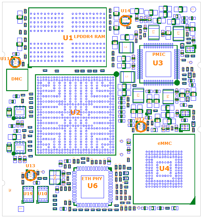
Temperature Sensor Locations
The TMP102 temperature sensor devices used are connected to the I2C1 bus. TMP102 measures temperatures from -40 °C to +125 °C. For a more detailed description of TMP102, refer to the Texas Instruments TMP102 Datasheet.
| Sensor | I2C slave address |
|---|---|
| U11 | 0x48 |
| U12 | 0x49 |
| U13 | 0x4A |
| U14 | 0x4B |
I2C1 Temperature Sensor Slave Addresses
CPU Core Frequency Scaling
The phyCORE-i.MX 8M Plus FPSC is able to scale the clock frequency and voltage. This is used to save power and reduce heat dissipation when the full performance of the CPU is not needed. Scaling the frequency and voltage is referred to as 'Dynamic Voltage and Frequency Scaling' (DVFS).
The phyCORE-i.MX 8M Plus FPSC BSP supports the DVFS feature. The Linux kernel provides a DVFS framework that allows each CPU core to have a min/max frequency as well as the applicable voltage and a governor that governs these values depending on the system load. Depending on the i.MX 8M Plus variant used, several different frequencies are supported. Further details on how to configure this governor can be found in the phyCORE-i.MX 8M Plus FPSC BSP Manual.
Technical Specifications
Warning
Due to changes in functionality and design that are currently being developed, several values cannot be determined in time for the release of this manual. All values with "TBD (To Be Determined)" are currently being evaluated. These values will be added to future manual editions.
The FPSC version has a profile of max. 5.5 mm thick, with a maximum component height of 2.0 mm on the bottom side of the PCB and approximately 1.5 mm on the top side. The board itself is approximately 2.0 mm thick. The phyCORE-8.MX 8M Plus FPSC DSC footprint can be seen below.
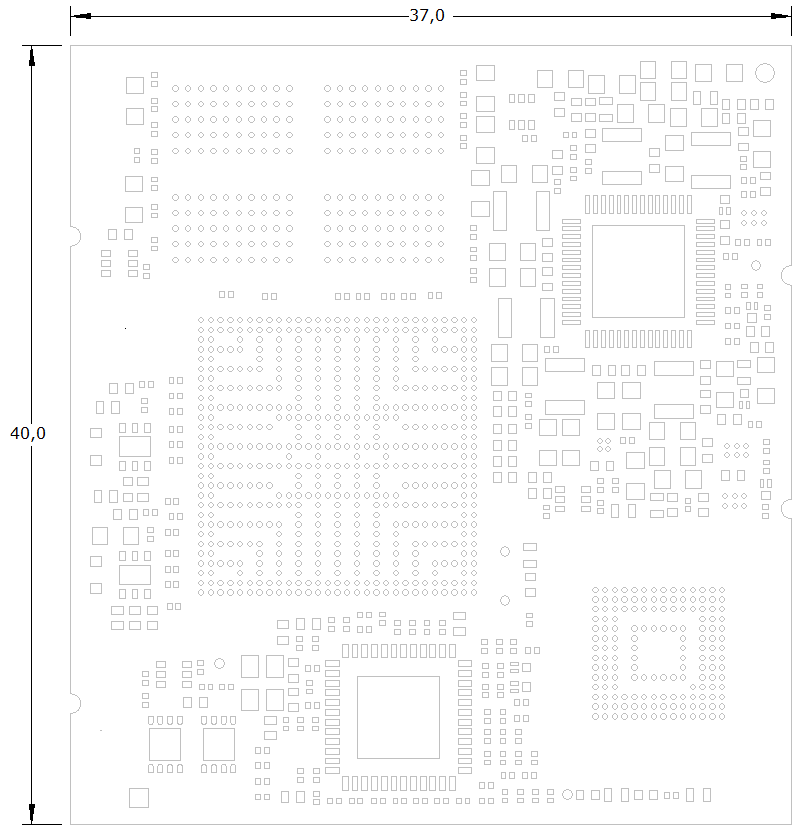
phyCORE-i.MX 8M Plus FPSC dimensions (top view; unit is mm)
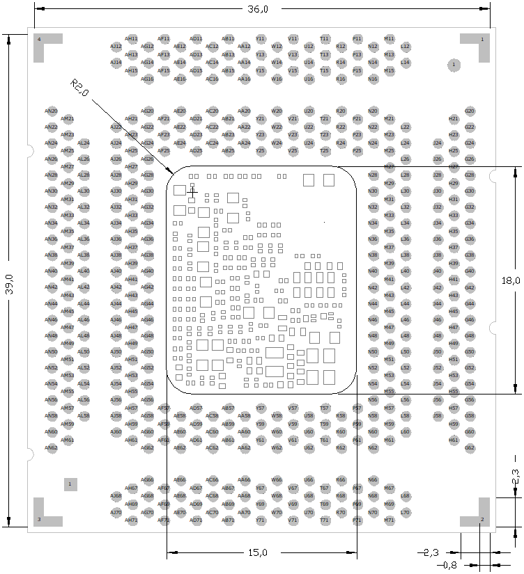
phyCORE-i.MX 8M Plus FPSC dimensions (bottom view top down; unit is mm)
Tip
For a downloadable version of the phyCORE-i.MX 8M Plus FPSC mechanical data and dimensions, go to the download section of our product website:
https://www.phytec.de/produkte/system-on-modules/phycore-imx-8m-plus-fpsc/#downloads
For FPSC Baseboard Footprint definitions as well as numbering schema, please refer to the corresponding FPSC Gamma Feature Set Specifications (LAN-118e.A6).
Additional specifications:
| Dimensions: | 40 x 37 mm |
| Weight: | ca. 8g |
| Storage Temperature: | -40 to +85 °C |
| Operating Temperature: | Product Temperature Grades |
| Humidity: | 10 % - 90 % (non-condensing) |
| Operating Voltage: | 4.75 V .. 5.25 V |
| Power Consumption: | phyCORE-i.MX 8M Plus FPSC Power Consumption |
Technical Specifications
These specifications describe the standard configuration of the phyCORE‑i.MX 8M Plus FPSC as of the printing of this manual.
phyCORE-i.MX 8M Plus FPSC Power Consumption
The values listed in the table below are guidelines to determine the required dimensions of the power supply circuitry on a carrier board. They do not take application-specific load situations into account. These values have been generated by looking at the maximum power consumption measured using different load scenarios and adding a voltage source of 3.3 V. These values are based on internal PHYTEC testing. Customers need to consider their application power requirements to ensure they do not generate a load greater than the values listed here.
| Required Supply Voltage | 5.0 V |
| Ramp-Up Time (10 %-90 %) | 100 µs to 10 ms |
| Allowed Tolerance of Supply Voltage | 4.75 V .. 5.25 V (Abs. max 5.5 V) |
| Max. current consumption | 2.5 A |
phyCORE-i.MX 8M Plus Power FPSC Consumption
For power measurement, a SOM (PCL-078) with 2 GB RAM, 8GB eMMC, ETH0, HDMI, and an IMX8ML8DVNLZAA was used together with PD23.1.0.
| Case 1 | Case 2 | Case 3 | Case 4 | Case 5 | Case 6 | |
|---|---|---|---|---|---|---|
| eMMC-Boot system idle DVFS ondemand | X | X | X | X | X | X |
| iperf3 client eth0 (~900MBit/s) | X | X | X | X | X | |
| CPU-Load (4x dd from /dev/urandom to /dev/null) | X | X | X | X | ||
| RAM-Load (memtester) | X | X | X | |||
| GPU-Load (qt5-opengles2-test) | X | |||||
VPU-Load (video 1080p) | X | |||||
| Power Consumption [Watt] | ||||||
| CPU Thermal Zone 0 [°C] | ||||||
| CPU Thermal Zone 1 [°C] | ||||||
| CPU Surface Temperature [°C] | ||||||
| RAM Surface Temperature [°C] | ||||||
| Eth-PHY Surface Temperature [°C] | ||||||
| PMIC Surface Temperature [°C] | ||||||
| Ambient [°C] |
phyCORE-i.MX 8M Plus FPSC Power Consumption Test Scenarios
Additionally, some values cannot be tested. Situations such as suspending to RAM, suspend freeze, and standby mode must be tested on a case-by-case basis to ensure the application's power consumption stays within the guidelines stated above.
Tip
For further information and assistance regarding your application's power consumption, please contact PHYTEC sales.
Product Temperature Grade | Controller Range | RAM (Case Temperature) | Other (Ambient) |
|---|---|---|---|
I | Industrial: -40 °C to +105 °C | Industrial: -40 °C to +95 °C | Industrial: -40 °C to +85 °C |
C | Commercial: 0 °C to +95 °C | Consumer: 0 °C to +95 °C | Consumer: 0 °C to +70 °C |
Product Temperature Grades
FPSC Footprint on the phyCORE-i.MX 8M Plus FPSC
For information on the footprint, mating baseboard footprint, numbering schema, etc. please refer to the corresponding FPSC Gamma Feature Set Specifications (LAN-118e.A6).
Pin numbering schema:
FPSC Gamma Feature Set Specifications (LAN118e.A6) - Pin Numbering
Mating FPSC Baseboard Footprint;
FPSC Gamma Feature Set Specifications (LAN118e.A6) - Baseboard
Interface Signal Trace Length
PHYTEC recommends a control delay and trace length of the high-speed interface signals. Signal delay and trace length of the high-speed interface signals routed on the phyCORE‑i.MX 8M Plus FPSC are listed in the following table. Take these values into consideration for the calculation of the overall delay and trace length budgets.
| Signal | Delay [ps] | Length [mm] | Signal | Delay [ps] | Length [mm] |
| X_MIPI_CSI1_CLK_N | 138 | 20,10 | X_LVDS1_CLK_N | 224 | 32,01 |
| X_MIPI_CSI1_CLK_P | 137 | 20,06 | X_LVDS1_CLK_P | 223 | 31,91 |
| X_MIPI_CSI1_D0_N | 132 | 19,87 | X_LVDS1_D0_N | 224 | 31,99 |
| X_MIPI_CSI1_D0_P | 132 | 19,88 | X_LVDS1_D0_P | 222 | 31,95 |
| X_MIPI_CSI1_D1_N | 136 | 19,84 | X_LVDS1_D1_N | 216 | 31,85 |
| X_MIPI_CSI1_D1_P | 136 | 19,83 | X_LVDS1_D1_P | 217 | 31,85 |
| X_MIPI_CSI1_D2_N | 137 | 19,93 | X_LVDS1_D2_N | 222 | 31,94 |
| X_MIPI_CSI1_D2_P | 137 | 19,95 | X_LVDS1_D2_P | 223 | 31,96 |
| X_MIPI_CSI1_D3_N | 136 | 19,81 | X_LVDS1_D3_N | 223 | 32,04 |
| X_MIPI_CSI1_D3_P | 136 | 19,81 | X_LVDS1_D3_P | 222 | 31,93 |
| X_MIPI_CSI2_CLK_N | 167 | 24,13 | X_PCIE_REF_PAD_CLK_N | 249 | 36,61 |
| X_MIPI_CSI2_CLK_P | 166 | 24,08 | X_PCIE_REF_PAD_CLK_P | 248 | 36,58 |
| X_MIPI_CSI2_D0_N | 168 | 24,22 | X_PCIE_RXN_N | 254 | 36,64 |
| X_MIPI_CSI2_D0_P | 166 | 24,17 | X_PCIE_RXN_P | 254 | 36,64 |
| X_MIPI_CSI2_D1_N | 167 | 24,08 | X_PCIE_TXN_N | 251 | 36,68 |
| X_MIPI_CSI2_D1_P | 166 | 24,06 | X_PCIE_TXN_P | 251 | 36,67 |
| X_MIPI_CSI2_D2_N | 167 | 24,17 | X_QSPIA_DQ0 | 255 | 37,50 |
| X_MIPI_CSI2_D2_P | 167 | 24,17 | X_QSPIA_DQ1 | 288 | 42,33 |
| X_MIPI_CSI2_D3_N | 167 | 24,17 | X_QSPIA_DQ2 | 286 | 41,19 |
| X_MIPI_CSI2_D3_P | 166 | 24,17 | X_QSPIA_DQ3 | 265 | 38,17 |
| X_MIPI_DSI1_CLK_N | 211 | 30,22 | X_QSPIA_SCLK | 280 | 41,14 |
| X_MIPI_DSI1_CLK_P | 211 | 30,23 | X_QSPIA_SS0 | 273 | 39,27 |
| X_MIPI_DSI1_D0_N | 207 | 30,32 | X_ENET_RGMII_RD0 | 16 | 2,38 |
| X_MIPI_DSI1_D0_P | 207 | 30,32 | X_ENET_RGMII_RD1 | 11 | 1,61 |
| X_MIPI_DSI1_D1_N | 208 | 30,15 | X_ENET_RGMII_RD2 | 20 | 2,95 |
| X_MIPI_DSI1_D1_P | 209 | 30,16 | X_ENET_RGMII_RD3 | 17 | 2,51 |
| X_MIPI_DSI1_D2_N | 210 | 30,32 | X_ENET_RGMII_RX_CTL | 18 | 2,76 |
| X_MIPI_DSI1_D2_P | 210 | 30,32 | X_ENET_RGMII_RXC | 22 | 3,40 |
| X_MIPI_DSI1_D3_N | 211 | 30,22 | X_ENET_RGMII_TD0 | 98 | 14,90 |
| X_MIPI_DSI1_D3_P | 209 | 30,18 | X_ENET_RGMII_TD1 | 100 | 15,05 |
| X_ETH_A_N | 116 | 16,70 | X_ENET_RGMII_TD2 | 110 | 17,08 |
| X_ETH_A_P | 116 | 16,74 | X_ENET_RGMII_TD3 | 106 | 16,02 |
| X_ETH_B_N | 117 | 16,71 | X_ENET_RGMII_TX_CTL | 113 | 17,32 |
| X_ETH_B_P | 117 | 16,84 | X_ENET_RGMII_TXC | 104 | 15,53 |
| X_ETH_C_N | 116 | 16,66 | X_SD1_CLK | 243 | 37,46 |
| X_ETH_C_P | 116 | 16,77 | X_SD1_CMD | 269 | 41,98 |
| X_ETH_D_N | 116 | 16,74 | X_SD1_DATA0 | 263 | 41,04 |
| X_ETH_D_P | 116 | 16,71 | X_SD1_DATA1 | 269 | 41,43 |
| X_HDMI_CEC | 260 | 38,32 | X_SD1_DATA2 | 266 | 41,60 |
| X_HDMI_DDC_SCL | 232 | 33,67 | X_SD1_DATA3 | 267 | 41,09 |
| X_HDMI_DDC_SDA | 245 | 35,54 | X_SD1_DATA4 | 270 | 42,06 |
| X_HDMI_EARC_AUX | 252 | 37,34 | X_SD1_DATA5 | 264 | 41,21 |
| X_HDMI_EARC_N_HPD | 258 | 37,36 | X_SD1_DATA6 | 269 | 41,98 |
| X_HDMI_EARC_P_UTIL | 258 | 37,36 | X_SD1_DATA7 | 267 | 41,51 |
| X_HDMI_HPD | 249 | 36,59 | X_SD1_STROBE | 221 | 32,25 |
| X_HDMI_TX0_N | 257 | 37,13 | X_SD2_CLK | 155 | 22,63 |
| X_HDMI_TX0_P | 257 | 37,12 | X_SD2_CMD | 178 | 25,96 |
| X_HDMI_TX1_N | 260 | 37,51 | X_SD2_DATA0 | 178 | 25,91 |
| X_HDMI_TX1_P | 259 | 37,44 | X_SD2_DATA1 | 180 | 26,12 |
| X_HDMI_TX2_N | 261 | 37,68 | X_SD2_DATA2 | 186 | 26,98 |
| X_HDMI_TX2_P | 260 | 37,60 | X_SD2_DATA3 | 182 | 26,41 |
| X_HDMI_TXC_N | 256 | 37,06 | X_USB1_D_N | 139 | 20,35 |
| X_HDMI_TXC_P | 256 | 37,06 | X_USB1_D_P | 140 | 20,47 |
| X_LVDS0_CLK_N | 130 | 18,94 | X_USB1_RX_N | 192 | 27,87 |
| X_LVDS0_CLK_P | 128 | 18,97 | X_USB1_RX_P | 192 | 27,87 |
| X_LVDS0_D0_N | 132 | 19,16 | X_USB1_TX_N | 315 | 46,02 |
| X_LVDS0_D0_P | 131 | 19,16 | X_USB1_TX_P | 314 | 46,08 |
| X_LVDS0_D1_N | 131 | 18,95 | X_USB2_D_N | 114 | 16,75 |
| X_LVDS0_D1_P | 130 | 19,02 | X_USB2_D_P | 115 | 16,86 |
| X_LVDS0_D2_N | 131 | 18,95 | X_USB2_RX_N | 166 | 24,11 |
| X_LVDS0_D2_P | 129 | 18,99 | X_USB2_RX_P | 167 | 24,21 |
| X_LVDS0_D3_N | 132 | 19,06 | X_USB2_TX_N | 236 | 34,92 |
| X_LVDS0_D3_P | 130 | 19,02 | X_USB2_TX_P | 236 | 34,85 |
Interface Signal Trace Length Table
Hints for Integrating and Handling the phyCORE‑i.MX 8M Plus FPSC
Integrating the phyCORE-i.MX 8M Plus FPSC
Besides this hardware manual, more information is available to facilitate the integration of the phyCORE‑i.MX 8M Plus FPSC into customer applications.
- The design of the phyBOARD‑Pollux can be used as a reference for any customer application.
- Many answers to common questions can be found at: https://www.phytec.de/produkte/system-on-modules/phycore-imx-8m-plus-fpsc/#downloads/
- The link “Carrier Board” within the category Dimensional Drawing leads to the layout data phyCORE-i.MX 8M Plus FPSC Footprint. It is available in different file formats. The use of this data allows the user to integrate the phyCORE-i.MX 8M Plus FPSC SoM as a single component in their design.
- Different support packages are available for support in all stages of embedded development. Please visit https://www.phytec.de/support/support-pakete/ or https://www.phytec.eu/support/support-packages/ or contact our sales team for more details.
Handling the phyCORE-i.MX 8M Plus FPSC
phyCORE Module Modifications
The removal of various components, such as the microcontroller or the standard quartz, is not advisable given the compact nature of the module. Should this nonetheless be necessary, please ensure that the board, as well as surrounding components and sockets, remain undamaged while desoldering. Overheating the board can cause the solder pads to loosen, rendering the module inoperable. If soldered components need to be removed, the use of a desoldering pump, desoldering braid, an infrared desoldering station, desoldering tweezers, a hot air rework station, or other desoldering methods is strongly recommended. Follow the instructions carefully for whatever method of removal is used.
Warning
If any modifications to the module are performed, regardless of their nature, the manufacturer's guarantee may be null and void.
Integrating the phyCORE into a Target Application
Successful integration in the user target circuitry greatly depends on adherence to the layout design rules for the GND connections of the phyCORE module. For maximum EMI performance, PHYTEC recommends, as a general design rule, connecting all GND pins to a solid ground plane.
Tip
Specific details may need to be considered when designing a customer-specific carrier board. For design information on carrier board components, please check the Design Considerations in each component section of phyCORE-i.MX 8M Plus FPSC on the Libra Development Board and the Design-In Guide - FPSC Gamma Featureset (LAN-123e.A2).
Ordering Information
The part numbering of the phyCORE PCL-078 has the following structure:
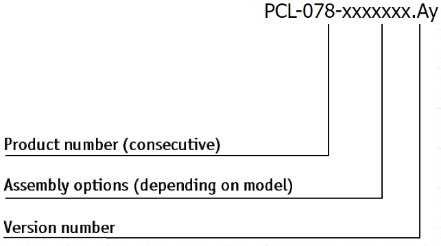
Product Specific Information and Technical Support
In order to receive product-specific information on all future changes and updates, we recommend registering at:
http://www.phytec.de/support/registrierung.html or http://www.phytec.eu/europe/support/registration.html
For technical support and additional information concerning your product, please visit the support section of our website, which provides product-specific information, such as errata sheets, application notes, FAQs, etc.
https://www.phytec.de/produkte/system-on-modules/phycore-imx-8m-plus-fpsc/
or
https://www.phytec.eu/en/produkte/system-on-modules/phycore-imx-8m-plus-fpsc/
phyCORE-i.MX 8M Plus FPSC on the Libra Development Board
Hardware Overview
The Libra Development Board for phyCORE-i.MX 8M Plus FPSC is a low-cost, feature-rich software development platform supporting the NXP Semiconductors i.MX 8M Plus microcontroller. Due to numerous standard interfaces, the Libra Development Board can serve as the bedrock for any application. At the core of the Libra Development Board is the PCL-078/phyCORE-i.MX 8M Plus FPSC System On Module (SOM) containing the processor, LPDDR4 RAM, eMMC Flash, power regulation, supervision, transceivers, and other core functions required to support the i.MX 8M Plus processor. Surrounding the SOM is the Libra Development Board, adding power input, buttons, connectors, signal breakout, and Ethernet connectivity, along with other peripherals.
Libra Development Board Concept
PHYTEC phyCORE carrier boards are fully equipped with all mechanical and electrical components necessary for a fast, secure start-up. Subsequent communication to and programming of applicable PHYTEC System on Modules (SoM) is made easy. phyCORE carrier boards are designed for evaluation, testing, and prototyping of PHYTEC System on Modules in laboratory environments prior to their use in customer-designed applications.
This modular development platform concept includes the following components:
- The phyCORE-i.MX 8M Plus FPSC Module populated with the i.MX 8M Plus microcontroller and all applicable SoM circuitry such as LPDDR4 SDRAM, eMMC-Flash, Ethernet-PHY, PMIC, etc.
- The Libra Development Board Carrier Board offers all essential components and connectors for a start-u,p including a power supply for 24 V input voltage and interface connectors such as HDMI, USB, and Ethernet, which enable the use of the SOM’s interfaces with a standard cable.
The carrier board can also serve as a reference design for developing custom target hardware in which the phyCORE SoM can be deployed. Carrier board schematics are available under a Non-Disclosure Agreement (NDA). The reuse of carrier board circuitry enables users of PHYTEC SoMs to shorten time-to-market, reduce development costs, and avoid substantial design issues and risks.
SBCplus Concept
The SBCplus concept was developed to meet the many, small differences in customer requirements with little development effort. This greatly reduces the time-to-market. The core of the SBCplus concept is the SBC design library (a kind of construction set) that consists of a large number of function blocks (so-called "building blocks") that are continuously being refined and updated.
Recombining these function blocks allows PHYTEC to develop a customer-specific SBC within a short time. We are able to deliver production-ready custom Single Board Computers within a few weeks at very low costs. The already developed SBCs, such as the phyBOARD-Pollux, each represent a combination of different customer wishes. This means all necessary interfaces are already available on the standard versions, allowing PHYTEC SBCs to be integrated into a large number of applications without modification.
For any necessary detail adjustment, extension connectors are available which enable a wide variety of functions to be added.
Tip
For further information, please contact PHYTEC sales.
1x USB-Host interface made available through a USB 3.0 4-port HUB at: USB 3.0 Type-A connector (Actual USB speed depends on mounted SoM) Mini PCI express connector (USB 2.0) Audio/Video connector (USB 2.0) Expansion Connector (USB 2.0)[2] COMING SOON There are several SoMs that can be used with the Libra Development Board. Below is a comprehensive list of features that each SoM contains and can be used with the Libra Development Board. For more information, please contact your PHYTEC representative (Contact Information). x x x x x x Most components on the Libra Development Board have an operating temperature range of -40 °C to 85 °C. The following components are the exception: For this reason, the operation temperature range for the kit variant is: -25 °C to 70 °C. The storage temperature range is -40 °C to 85 °C. For detailed dimensions, refer to the provided CAD data (e.g. DXF file) in the download section of our specific FPSC SoMs: Libra Development Board Components Tip For high-resolution pictures of the Libra Development Board, please go to the download section of our specific FPSC SoMs. Note For easy reference, Pin 1 for each component has been highlighted. The Libra Development Board features many interfaces and is equipped with the components listed in the table Connectors and Pin Header. For a more detailed description of each component, refer to the appropriate section listed in the table below. Libra Development Board Components (Top) and Libra Development Board Components (Bottom) highlight the location of each component for easy identification. The table below lists all available connectors on the Libra Development Board. Reference Designator Description Section Warning Ensure that all module connections do not exceed their expressed maximum voltage or current. Maximum signal input values are indicated in the corresponding controller User's Manual/Data Sheets. As damage from improper connections varies according to use and application, the user must take appropriate safety measures to ensure that the module connections are protected from overloading through connected peripherals. The Libra Development Board is populated with 7 LEDs. Libra Development Board Components (Top) and Libra Development Board Components (Bottom) show the location of the LEDs. Their functions are listed in the table below: LED Color Description Section D6 The Libra Development Board is populated with multiple switches and buttons. The table below shows their functions: RS485 termination switch UART1 target switch CAN FD1 termination switch CAN FD2 termination switch The Libra Development Board comes pre-configured with several removable jumpers (JP) and solder jumpers (J). These jumpers enable the flexible configuration of a limited number of features for development purposes. Warning Due to the small footprint of the solder jumpers (J), PHYTEC does not recommend manual jumper modifications. This may also render the warranty invalid. Only the removable jumper (JP) is described in this section. Contact our sales team if you need jumper configurations different from the default configuration. The function of the removable jumper on the Libra Development Board is shown below. More detailed information can be found in the appropriate section. 1+2 5+6 UART2_RXD - USB Debug 2 This section provides a more detailed look at the Libra Development Board components. Each subsection details a particular connector/interface and associated jumpers for configuring that interface. Tip Where possible, we also provide useful information regarding design considerations for components. This can be used if you plan to design your own carrier board. Warning Do not change modules or jumper settings while the Libra Development Board is supplied with power! The Libra Development Board can be powered either by a 2-pole Phoenix Contact MINI COMBICON base strip 3.5 mm connector (X8) or by a USB Power Delivery Supply (X2). Warning Do not power the Libra Development Board via X2 and X8 at the same time! The Libra Development Board is available with one power supply connector, a 2-pole Phoenix Contact MINI COMBICON base strip 3.5 mm connector (X8) suitable for a single 24 V supply voltage. The required current load capacity for all power supply solutions depends on the specific configuration of the phyCORE mounted on the Libra Development Board, the particular interfaces enabled while executing software, as well as whether an optional expansion board is connected to the carrier board. The permissible input voltage is 24 V DC if your SBC is equipped with a 2-pole Phoenix Contact MINI COMBICON base strip. A 24 V power supply capable of providing at least (TBD A) is recommended to power the board via the 2-pole base strip. The pin assignment for power supply connector X2: Description The Libra Development Board can be powered by a USB Power Delivery Supply. The Libra Development Board provides the needed voltage and current with the connected supply and enables the on-board voltages. A 100 W USB-PD supply is recommended to power the Libra Development Board. Note Please note that connector X8 is only usable as a power supply input. It doesn't offer any USB communication interface functionality. The Libra Development Board has a double-layer capacitor equipped to back up the VDD_RTC rail of the phyCORE FPSC SoM. The mounted 330 mF capacitor is capable of backing up the SoM RTC for at least (TBD) at 25 °C. The Libra Development Board features 3 UART interfaces. This paragraph describes their default and alternative purposes. UART1 (full flow control) is configurable to provide one of three functions via 2 integrated (U38/U40) and one hardware switch S5. The following table explains the necessary settings for a desired UART1 target: UART2 (full flow control) is connected to the USB debug channel 2 via the default setting of JP1. UART3 is connected to the USB debug channel 1 via the default setting of JP1. When designing a custom carrier board, remember the TTL level is 1.8 V. Pin header connector X27 provides the UART1 signals of the phyCORE FPSC SoM at either RS-232 or RS-485 level. Mode is selected by routing UART1 to the applicable converter. Please refer to UART1 Target Selection. The RS-232 interface is intended to be used as data terminal equipment (DTE) and allows for a 5-wire connection, including the signals RTS and CTS for hardware flow control. RS-485 is available in Half-Duplex (3-wire). The table below shows the signal mapping of the RS-232 and RS-485 level signals at connector X27. Interface Pin # Signal Name Signal Type Signal Level Description The phyCORE FPSC SoM FLEXCAN1 and FLEXCAN2 interfaces are brought out at X29 and X31, each as CAN FD. The maximum permissible CAN FD data rate is 8 Mbit/s. For development purposes, a 120 Ω termination can be added by closing SW5 (CAN1) or SW6 (CAN2). For standard use, it is possible to mount a more suitable split termination in a customer-specific BOM. The pinout is chosen to fit the official standard CAN pinout and is displayed in the table below. on a DE-9 plug (D-Sub 9 pin), where CAN_L is pin 2, CAN_H is pin 7, GND is pin 3, and VCC_5V is pin 9. Interface Pin # Signal Name Signal Type Signal Level Description Interface Pin # Signal Name Signal Type Signal Level Description The Libra Development Board is equipped with 3 RJ45 connectors. The table below describes the properties of each Ethernet interface: Ethernet Connector Interface Description 10/100/1000/2500/5000/10000 MBit/s Ethernet interface over 6-speed Ethernet transceiver on carrier board The LEDs for LINK (green) and ACTIVITY (orange) indications are integrated into the connector. The Ethernet transceivers support Auto MDI-X, eliminating the need for a direct connect LAN or cross-over path cable. They detect the TX and RX pins of the connected device and automatically configure the PHY TX and RX pins accordingly. The data lanes should be routed with a differential impedance of 100 Ohm. The center taps of each pair's transformer have to be connected to GND through a 100nF capacitor. The LED pins are open-drain outputs of the SoM without a resistor, so they should be connected to the cathodes of the LEDs through a resistor. The Libra Development Board provides a USB 3.0 interface at the USB Type-A connector X16. It is a Host interface made available through a 4-port USB HUB. The Libra Development Board provides a USB-C 3.2 GEN 1(10 Gbps) interface. The USB Serial Downloader requires this interface to be able to boot from USB. The lower socket is connected via a USB 3.2 Gen 1 hub to USB2 of the phyCORE FPSC SoM. Series capacitors are already present on the phyCORE FPSC SoM. It is not necessary to provide additional series capacitors in the TX lines. Double-check the signal direction of the high-speed lines where TX is output and RX is input on phyCORE FPSC SoM. The TX and RX lines should be routed with an impedance of 50 Ohms to a ground plane and 100 Ohms differential impedance. Route USB D lines with 45 Ohms to Ground and 90 Ohms differential impedance. The primary debug interface is UART3. UART4 is the debug interface for the M7 core. Both UART interfaces are connected to a UART-to-USB Converter (U15 FTDI FT4232H). The USB interface is brought out at a USB-C socket (X14). Use the following terminal settings to connect to Libra Development Board serial interfaces: The USB debug interface is also capable of manipulating the Boot Mode signals through FT4232H bank D and triggering a reset through FT4232H bank C. The table below shows the pinout of the USB Debug connector: Interface Pin # Signal name Signal Type Signal Level Description The Libra Development Board provides a standard microSDHC card slot at X60 for use with SD/MMC interface cards. It allows for a fast, easy connection to peripheral devices like microSD and MMC cards. Power to the SD interface is supplied by inserting the appropriate card into the SD/MMC connector. It also features card detection, a lock mechanism, and a smooth extraction function by pushing the card in and out. Series resistors might be required to adapt the drive strength of the card. SD interface should be routed with an impedance of 50 Ohms to a ground plane. The trace length between CLK, CMD, and DATA lanes should be matched and kept as short as possible. Avoid Vias and take care of the signal current return path. The 1-lane PCI Express interface provides PCIe Gen. 3.0 functionality, which supports up to 8 GT/s operations. Various control signals are implemented with GPIOs. The PCIE1 interface is brought out at the Mini PCIe connector X52 shown above. The PCIe clock is generated by the dedicated PCIe clock generator U51. The table below shows in-depth information, such as pin assignment and signals used to implement special features of the Mini PCIe interface. Interface Pin # Signal name Signal Type Signal Level Description 100nF AC coupling capacitors are placed at the output of the phyCORE FPSC SoM in series to the TX lanes. A clock generator on the carrier board generates the PCIe clock. The second 1-lane PCI Express interface provides PCIe Gen. 3.0 functionality, which supports up to 8 GT/s operations. The mounted M.2 Key-M connector is mainly used for SSD cards. Various control signals are implemented with GPIOs. The PCIE2 interface is brought out at the M.2 Key-M connector X54 shown above. The PCIe clock is generated by the dedicated PCIe clock generator U51. The M.2 Key-M connector is only available with the FPSC SoM PCL-079 The table below shows in-depth information, such as pin assignment and signals used to implement special features of the M.2 Key-M interface. Interface Pin # Signal name Signal Type Signal Level Description The phyCORE FPSC SoM on the Libra Development Board offers 2 independent interfaces to connect digital camera boards with the MIPI CSI-2 interface. The 4-lane MIPI CSI-2 interfaces are brought out as phyCAM-M camera interfaces at connectors X32 and X34. The pin assignments of connectors X32 and X34 are shown below. The phyCAM-M camera connectors fit the phyCAM-M product family with different colors and monochrome sensors. Suitable camera modules are e.g. VM-016-COL-M (1 MPix) or VM-017-BW-M (5 Mpix), which can be delivered with a complete objective. Contact the PHYTEC Sales Team for advice on how to tailor a camera module to your application. The suitable cable can be found in the table below. Interface Pin # Signal name Signal Type Signal Level Description Interface Pin # Signal name Signal Type Signal Level Description Regarding camera connections when designing a customer carrier board: General information and design guidelines for PHYTEC camera interfaces can be found here: Specific information for each PHYTEC camera module can be found on that module's download page: PHYTEC Embedded Vision (Deutsch) or PHYTEC Embedded Vision (English). The Libra Development Board provides a High-Definition Multimedia Interface (HDMI), which is compliant with HDMI 2.0a. It supports a maximum resolution of 1920x1080p60, 1280x720p60, 720x480p60, and 640x480p60. Please refer to the applicable phyCORE FPSC SoM Applications Processor Reference Manual for more information. This feature is not available for all mountable FPSC SoMs. The HDMI interface is brought out at a standard HDMI type A connector (X20) on the Libra Development Board and comprises the following signal groups: All signals are routed from the phyCORE‑Connector to the HDMI receptacle through ESD Protection Diodes. Interface Pin # Signal name Signal Type Signal Level Description 1 2 GND - - Ground 3 4 5 GND - - Ground 6 7 8 GND - - Ground 9 10 11 GND - - Ground 12 13 14 15 16 17 GND - - Ground 18 19 20 - - 21 - - 22 - - 23 - - The differential impedance should be 100 Ohms for all lanes to a Ground Plane. The lanes should be matched. The DDC lanes need pull-up resistors between 1.5k and 2k to 5V through a diode. The CEC lane needs a 27k pull-up resistor connected to 3.3 V through a diode. This prevents leaking current in a power-off state. The phyCORE FPSC SoM offers one LVDS display interface that supports two output channels. The Audio/Video (A/V) connectors X46 and X50 provide an easy way to add typical A/V functions and features to the Libra Development Board. Standard interfaces such as 4-lane LVDS, I2S, I2C, and USB, as well as different supply voltages, are available at the two A/V female dual-entry connectors. A special feature of these connectors is their connectivity from the top or bottom. The A/V connector is intended to be used with phyBOARD Expansion Boards and to add specific audio/video connectivity with custom expansion boards. A/V connector X46 makes all signals for display connectivity available, while X50 provides signals for audio and touchscreen connectivity as well as an I2C bus and additional control signals. The tables below show the pin assignment of connectors X46 and X50. Interface Pin # Signal name Signal Type Signal Level Description 1 GND - - Ground 2 - 3 - 4 5 6 GND - - Ground 7 GND - - Ground 8 - 9 - 10 11 12 GND - - Ground 13 GND - - Ground 14 - 15 16 Interface Pin # Signal name Signal Type Signal Level Description GND - - Ground GND - - Ground GND - - Ground GND - - Ground GND - - Ground The differential impedance of LVDS2 lanes should be 100 Ohm and 50 Ohm to a ground plane for all lanes. Lanes should be matched. The audio signals should have a single-ended impedance of 50 Ohms to a ground plane. The phyCORE FPSC SoM offers one LVDS display interface that supports two output channels. The video connectors X43 and X44 provide an easy way to connect a display to the Libra Development Board. The pinout of both connectors fits the Glyn LVDS Display Family with different display sizes and display resolutions. In addition to the Glyn LVDS signals, there are USB and I²C for touch brought out at X34 as well. The connectors are intended to be used with PHYTEC KLCD-AC163. The tables below show the pin assignment of connectors X43 and X44. Interface Pin # Signal name Signal Type Signal Level Description Interface Pin # Signal name Signal Type Signal Level Description The differential impedance of LVDS0 lanes should be 100 Ohm and 50 Ohm to a Ground-Plane for all lanes. The lanes should be matched. The phyCORE-i.MX 8M Plus FPSC offers one MIPI-DSI display interface (not available on phyCORE-i.MX 95 FPSC). MIPI-DSI has 4 channels, supporting one display with a resolution of up to 1920 x 1080 at 60Hz. The following table shows the pin assignment of connector X39 (Hirose DF12(4.0)-36DP-0.5V(86)). Interface Pin # Signal name Signal Type Signal Level Description The differential impedance of MIPI-DSI1 lanes should be 100 Ohms and 50 Ohms to a ground plane for all lanes. The lanes should be matched. The expansion connector X56 provides an easy way to add other functions and features to the Libra Development Board. Standard interfaces such as SPI, USB, JTAG, UART, SDIO, and I2C are available at the expansion connector. The expansion connector is intended to be used with a phyBOARD Evaluation Adapter. The expansion connector can also add specific functions with custom expansion boards. Information on the Evaluation Adapter for the expansion connector can be found in the Application Guide for phyBOARD Expansion Boards (phyBOARD-Wega Expansion Guide (L-793_0)). The pinout of the expansion connector is shown in the table below: Interface Pin # Signal name Signal Type Signal Level Description If heatsinking is required for the phyCORE FPSC SoM, a PWM-controlled fan can be connected to the Libra Development Board. The fan's supply voltage is 5 V, and the PWM signal is brought out as open drain. The frequency generator signal, which can be used to monitor fan rotation, is connected to test pad TP55 and comes with a pull-up resistor to 3.3 V. A Hirose DF13-4P-1.25V (75) socket is used as a connector with the following pinout: Interface Pin # Signal Name Signal Type Signal Level Description If heatsinking is required for the phyCORE FPSC SoM, a PWM-controlled fan can be connected to the Libra Development Board. The fan's supply voltage is 5 V, and the PWM signal is brought out as open drain. The frequency generator signal, which can be used to monitor fan rotation, is connected to test pad TP55 and comes with a pull-up resistor to 3.3 V. A Hirose DF13-4P-1.25V (75) socket is used as a connector with the following pinout: Interface Pin # Signal Name Signal Type Signal Level Description The Libra Development Board provides one multicolor (RGB) LED (D31). The LED is connected to an LED driver (NXP PCA9533/01) controlled by the I2C3 bus. The location for D31 can be found in LEDs. The Libra Development Board provides a 2 kbit EEPROM (ST M24C02-RMC6TG) for general use. It is controlled by the I2C2 bus. The EEPROM's write protection pin is connected to TP60. Write protection can be enabled by mounting an R333 pull-up resistor. In this case, the EEPROM can be written if TP60 is tied to Ground only. The EEPROM I²C address can be fully customized by jumpers J21, J22, and J23. The default address is 0x51. The Libra Development Board features a 512MBit Quad SPI NOR at U62. TBD TBD The Libra Development Board is equipped with a P3T1750DPZ I3C temperature sensor. TBD The X_nRESET_OUT signal (X_POR_B at phyCORE FPSC SoM) is used to hold all devices with an external reset pin in the reset state. X_nRESET_OUT will be released after all board voltages are powered up and allows the phyCORE FPSC SoM to boot. X_nRESET_OUT is brought out at several connectors like the Expansion Connector (X56). Note that there is a 10 kOhms pull-up resistor on the phyCORE FPSC SoM VDD_IO voltage. It is recommended to use this signal as an open drain. The Libra Development Board provides supply voltages on several connectors to power external devices. Be sure not to exceed the maximum permissible current that can be drawn from each power domain. In the table below, each source is listed with the location where a voltage connected to the source can be found: Note When utilizing one of the multiple ground studs for any purpose, keep in mind that stud X97 is connected to an isolated GND_DEBUG. In addition to these currents, Libra Development Board delivers current for USB_VBUS of X16/X18 (2x 900 mA), phyCAM-M Interfaces (2x 1500 mA 3.3 V or 5 V depending on VCC_SELECT pin), and HDMI connector (150 mA). Warning Drawing current may result in heating of the voltage regulator components and might require additional heat sinking. The input current of the SoM supply rail VDD_SOM can be measured on board to determine the power consumption of the SOM. A current sense amplifier translates the supply current into a proportional voltage VOUT_CC_SOM, which can be measured at X12 (on PCB top side) and X12 (on PCB bottom side). The mounted amplifier features a gain of 100V/V. The SoM input current ISOM_IN in Ampere is determined by inserting VOUT_CC_SOM into the following equation: ISHUNT = VOUT,AMP * 2.5 PSOM_IN = ISHUNT * VDDSOM For example, measuring 400 mV at X12, the input current will be 1 A. With a SoM input voltage of 5.0 V, the input PSOM_IN is 5 W. The Libra Development Board has several switches and buttons for various uses. The locations for all switches can be found in Switches and Buttons. The Libra Development Board is equipped with a system reset button at S2. Pressing this button will assert reset through a voltage supervisor U11 that will pull the X_nRESET_IN pin (X1 Pin Y21) of the phyCORE FPSC SoM low, causing the module to reset with a complete power cycle. The Libra Development Board is equipped with an ON/OFF button at S3 and is connected to X_ONOFF of the phyCORE FPSC SoM. For more information, refer to the applicable CPU's Reference Manual. The Libra Development Board features a boot switch with four individually switchable ports to select the phyCORE FPSC SoM default bootsource. The Boot_Mode signals may also be accessed through pin header X9. Descriptions of the various boot modes can be found in Boot Mode Selection. The available boot options differ depending on the mounted FPSC SoM. All available options are displayed in the table below: Mounted SoM Boot location/target BOOT_MODE S1 switch number PCL-079 (FPSC phyCORE-i.MX 8MP) PCL-079 (FPSC phyCORE-i.MX 95) Interface Pin # Signal Name Signal Type Signal Level Description Bootpin voltages should be valid when X_POR_B (X_nRESET_IN at Libra Development Board) is released. The I2C1 interface of the phyCORE FPSC SoM is not connected to the Libra Development Board. The table below lists the connectors and pins with I2C connectivity and on-board devices. The I²C addresses are hexadecimal in the 7-bit representation of the default Linux representation. I2C2 Interface Location or Address I2C3 Interface Location or Address I2C4 Interface Location or Address I2C5 Interface Location or Address To avoid conflicts when connecting external I2C devices to the Libra Development Board, the addresses of the onboard I2C devices must be considered. The table below lists the addresses already in use; the default address is printed in bold. The I²C addresses are hexadecimal in 7-bit representation, which is the default Linux representation.Libra Development Board Features
The Libra Development Board supports the following features:Block Diagram
Libra Development Board Block DiagramSoM Feature List on the Libra Development Board
phyFLEX-i.MX 95 phyFLEX-i.MX 8M Plus phyFLEX-STM32MP2 phyFLEX-AM62Lx phyFLEX-i.MX 93 phyFLEX-i.MX 91 phyFLEX i.MX952 phyFLEX SL2610 Featureset Gamma Gamma Gamma Gamma Light Gamma Gamma Light Gamma Gamma Lite Subclass 1 / 2 / 3 1 / 2 / 3 1 / 2 / 3 2 / 3 1 / 2 / 3 3 1 / 2 / 3 Mandatory Signals RGMII x x x x x x x x Ethernet x x x x x x x x USB 2.x x x x x x USB 2.x x x x x x x x x (via onboard HUB) LVDS x x x x x NA x NA MIPI-CSI-2 (2 or 4 lanes) x x x NA x NA x x (2 Lanes) SD Card x x x x x x x x QSPI x x x x x CAN(-FD) (2) x x x x x x x x UART+Flow (2) x x x x x x x x UART x x x x x x x x SPI+CS (2) x x x x x x x x I2C (2) x x x x x x x x PWM (2) x x x x x x x x SAI 2-Lane x x x x x x x x (w/o TDM) JTAG x x x x x x x x PWR_IN x x x x x x x x Control/Misc x x x x x x x x GPIO (4) x x x x x x x x Optional Signals USB 3.x (1-2) 1 2 1 0 0 0 0 0 LVDS 1 1 1 0 0 0 1 0 MIPI-DSI 1 1 1 1 1 0 1 1 MIPI-CSI (2 or 4 lanes) 1 1 0 0 0 0 1 ( 2 Lanes) 0 HDMI/eARC 0 1 0 0 0 0 0 0 PCIe 2-Lane (1-2) 2 1 1 0 0 0 1 0 CAN(-FD) 0 0 0 1 0 0 0 0 SDIO4 1 1 1 1 0 0 1 1 SPI+CS 1 1 1 1 0 0 1 0 I2C (1-2) 1 1 2 1 0 0 2 1 PWM (1-2) 0 2 2 2 0 0 2 2 ADC (1-8) 8 0 4 (5) 4 4 4 8 8 GPIO (1-3) 3 3 3 3 0 0 3 3 Specialized Signals 10G Ethernet 1 0 0 0 0 0 0 0 USB 3 SS Signals 1 0 1 (or PCIe) 0 0 0 0 0 GPIO 1 4 4 4 0 0 7 5 FPSC Gamma Feature Set SignalsTemperature Range
BOM No. Component Description Temperature Range Advice C111 Double layer capacitor for RTC Backup -25 °C to 70 °C X37 HDMI Connector -25 °C to 85 °C There is no replacement available X43 LVDS1 Data Connector -35 °C to 85 °C There is no replacement available X44 LVDS1 Backlight Connector -25 °C to 85 °C There is no replacement available X68 Fan Connector -35 °C to 85 °C X60 Micro SD-Card Slot -25 °C to 85 °C The SD-Card slot can be used in the range of -40 °C to 85 °C without mechanical changes Libra Development Board Component Temperature RangeMechanical Dimensions
Libra Development Board Component Placement Diagram
 Libra Development Board Components (Top)
 Libra Development Board Components (Bottom)
Libra Development Board Component Overview
Connectors and Pin Header
X1 SoM FPSC solder connection phyCORE Connector (X1) X2 Carrier board power in USB-C Power Supply (X2/X8) X3 VDD_5V0 current amp header (not mounted) X4 VDD_3V3 current amp header (not mounted) X5 VDD_1V8 current amp header (not mounted) X6 SoM 3,3 V output header (not mounted) X7 SoM 1,8 V output header (not mounted) X8 Carrier board power in 2-pin connector Power Supply (X2/X8) X9 Boot Mode influence header Boot Header (X9) X10 JTAG header voltage level 1,8 V JTAG (X10) X12 SoM input current amp header (not mounted) SoM Input Current Amp Header (X12) X14 USB-C-Debug USB Debug (X14) X16 USB-A 3.0 USB Type-A 3.0 Interface (X16) X18 USB-C 3.2 OTG USB-C 3.2 GEN 1 Interface (X18) X21 Ethernet 10G RJ-45
Ethernet (X21/X22/X25)X22 Ethernet Gigabit RJ-45 X25 Ethernet Gigabit RJ-45 X27 RS232/RS485 10-pin header RS-232/RS-485 (X27) X29 CAN-FD1 10-pin header
CAN FD (X29/X31)X31 CAN-FD2 10-pin header X32 phyCAM-M CSI1 phyCAM-M MIPI CSI Camera Connectors (X32/34) X34 phyCAM-M CSI2 X37 HDMI HDMI (X37) X39 MIPI-DSI 36-pin board-to-board MIPI-DSI (X39) X43 LVDS1 data connector
LVDS1 (X43/X44)X44 LVDS1 backlight connector X46 LVDS2 AV-Connector display data 16-pin header
Audio/Video (SAI2/LVDS0)X50 AV-Connector audio + control 30-pin header X52 Mini PCIe Mini PCIe (X52) X54 M.2 Key-M M.2 Key-M (X54) X56 Expansion Connector 60-pin Expansion Connector (X56) X60 Micro SD-Card receptacle Secure Digital Memory Card / MultiMedia Card (X60) X68 Fan Connector 4-pin Fan (X68) X71 SPI ADC input 10-pin header SPI ADC (X71) X73 ADC input 10-pin header ADC (X71) X74,X75,X76,X79,X88,X89,X92,X93,X96,X100,X101 GND Stud X97 Debug GND Stud (isolated) X105-X110 FPSC reserved 20-pin socket Libra Development Board Connectors and Pin HeadersLEDs
 Libra Development Board LEDs (Top)
 Libra Development Board LEDs (Bottom)
Green VDD_5V0 good indicator D7 Red VDD_3V3 good indicator D8 Blue VDD_1V8 good indicator D9 Green VDD_SOM good indicator D12 Red Debug USB-C VBUS good indicator D30 Yellow M.2 SSD activity indicator D31 RGB Multi-color LED user-controllable Multicolor (RGB) LED (D31) Libra Development Board LED DescriptionsSwitches and Buttons
 Libra Development Board Switch Locations
Switch Description Section S1 4-port Boot Mode Switch Boot Switch (S1) S2 Reset push button System Reset Button (S2) S3 ON/OFF push button System ON/OFF Button (S3) S4
ON: Bus is terminated with 120 Ω
OFF: Bus is not terminatedS5
ON: UART1 is converted to RS232
OFF: UART1 is converted to RS485S6
ON: Bus is terminated with 120 Ω
OFF: Bus is not terminatedS7
ON: Bus is terminated with 120 Ω
OFF: Bus is not terminatedLibra Development Board SwitchesJumpers
 Jumper (JP1)
Jumper Position Default Description Section JP1
3+4
11+12UART3_RXD - USB Debug 1
UART3_TXD - USB Debug 1
UART2_TXD - USB Debug 2
UARTLibra Development Board Jumper SettingsLibra Development Board SBC Component Detail
phyCORE Connector (X1)
 phyCORE Connector (X1)
Power Supply (X2/X8)
 Power Supply Connectors (X2/X8)
Interface Pin # Signal 1 VDD_IN_PWR_CON 24 V (TBD A) power supply (min./max. TBD) 2 GND Ground X2 Pin AssignmentUSB Power Delivery Connector (X8)
RTC Backup Supply
UART
UART1 Target S5 U38 U40 Bluetooth over PEB-WLBT-05 mounted to Expansion Connector (X56) X UART1_BT_RS_SEL = 1
Default = 0X RS232 at X27 through U37 1 UART1_BT_RS_SEL = 0 UART1_RS232_485_SEL = 1
S5 override GPIORS485 at X27 through U39 0 UART1_BT_RS_SEL = 0 UART1_RS232_485_SEL = 0
S5 override GPIOUART1 Target SelectionUART Design Considerations
RS-232/RS-485 (X27)
 RS-232 and RS-485 Connector (X27)
1 NC - - No connect 2 NC - - No connect 3 X_RS232_RXD I - RS232 receive data 4 X_RS232_RTS O - RS232 request to send 5 X_RS232_TXD O - RS232 transmit data 6 X_RS232_CTS I - RS232 clear to send 7 X_RS485_A I/O - RS485 non-inverted 8 X_RS485_B I/O - RS485 inverted 9 GND - 0.0 V Ground 10 NC - - No connect RS-232/RS-485 (X27) Pin AssignmentCAN FD (X29/X31)
 CAN FD (X29/X31)
1 NC - - No connect 2 NC - - No connect 3 X_CAN1_L CAN_I/O - Low-level CAN bus input/output line 4 X_CAN1_H CAN_I/O - High-level CAN bus input/output line 5 GND - 0.0 V Ground 6 NC - - No connect 7 NC - - No connect 8 GND - 0.0 V Ground 9 NC - - No connect 10 NC - - No connect CAN FD1 (X29) Pin Assignment1 NC - - No connect 2 NC - - No connect 3 X_CAN2_L CAN_I/O - Low-level CAN bus input/output line 4 X_CAN2_H CAN_I/O - High-level CAN bus input/output line 5 GND - 0.0 V Ground 6 NC - - No connect 7 NC - - No connect 8 GND - 0.0 V Ground 9 NC - - No connect 10 NC - - No connect CAN FD2 (X31) Pin AssignmentEthernet (X21/X22/X25)
 Ethernet Connectors (X21/X22/X25)
X21
(This feature is only available with FPSC SoM PCL-079)X22 10/100/1000 Ethernet interface over Gigabit Ethernet transceiver on carrier board X25 10/100/1000 Ethernet interface over Gigabit Ethernet transceiver on mounted SoM RJ45 Ethernet connectors X21/X22/X25Ethernet Design Consideration
USB Type-A 3.0 Interface (X16)
 USB Type-A 3.0 Connector (X16)
USB-C 3.2 GEN 1 Interface (X18)
 USB 3.2 Gen1 Connector (X18)
USB 3.2 Gen1 Design Considerations
USB Debug (X14)
 USB Debug Connector (X14)
A1 GND - 0.0 V Ground A2 NC - - No connect A3 NC - - No connect A4 VBUS I 5.0 V USB VBUS provided by Host A5 CC1 I/O - Configuration channel 5k1 pull down A6 X_DEBUG_USB_DP USB_I/O - USB Debug Data+ A7 X_DEBUG_USB_DM USB_I/O - USB Debug Data- A8 NC - - No connect A9 VBUS I 5.0 V USB VBUS provided by Host A10 NC - - No connect A11 NC - - No connect A12 GND - 0.0 V Ground B1 GND - 0.0 V Ground B2 NC - - No connect B3 NC - - No connect B4 VBUS I 5.0 V USB VBUS provided by Host B5 CC2 I/O - Configuration channel 5k1 pull down B6 X_DEBUG_USB_DP USB_I/O - USB Debug Data+ B7 X_DEBUG_USB_DM USB_I/O - USB Debug Data- B8 NC - - No connect B9 VBUS I 5.0 V USB VBUS provided by Host B10 NC - - No connect B11 NC - - No connect B12 GND - 0.0 V Ground 25 GND_DEBUG - - Ground Debug isolated 26 GND_DEBUG - - Ground Debug isolated 27 GND_DEBUG - - Ground Debug isolated 28 GND_DEBUG - - Ground Debug isolated 29 GND_DEBUG - - Ground Debug isolated 30 GND_DEBUG - - Ground Debug isolated X14 Pin AssignmentSecure Digital Memory Card / MultiMedia Card (X60)
 SD / MM Card Connector (X60)
SD / MM Card Design Considerations
Mini PCIe (X52)
 PCIe Connector (X52)
1 X_PCIE1_nWAKE O 3.3 V nWAKE 2 VDD_3V3 PWR_O 3.3 V Mini PCIe 3.3 V power rail 3 PCIE1_COEX1 O 3.3 V COEX1 4 GND - 0.0 V Ground 5 PCIE2_COEX2 O 3.3 V COEX2 6 VDD_1V5_MPCI PWR_O 1.5 V Mini PCIE 1.5 V power rail 7 X_PCIE1_nCLKREQ_3V3 I 3.3 V Inverted Clock Request 8 TP48 - - Test point 9 GND - 0.0 V Ground 10 TP49 - - Test point 11 X_PCIE1_CON_REFPAD_CLK_P PCIE_O - 100 MHz reference clock positive signal 12 TP50 - - Test point 13 X_PCIE1_CON_REFPAD_CLK_N PCIE_O - 100 MHz reference clock negative signal 14 TP51 - - Test point 15 GND - 0.0 V Ground 16 TP52 - - Test point 17 TP53 - - Test point 18 GND - 0.0 V Ground 19 TP54 - - Test point 20 NC - - No connect 21 GND - 0.0 V Ground 22 X_PCIE1_nPERST_3V3 O 3.3 V nPERST 23 X_PCIE1_RXN_N PCIE_I - SoM receive negative signal 24 VDD_3V3 PWR_O 3.3 V Mini PCIe 3.3 V power rail 25 X_PCIE1_RXN_P PCIE_I - SoM receives a positive signal 26 GND - 0.0 V Ground 27 GND - 0.0 V Ground 28 VDD_1V5_MPCI PWR_O 1.5 V Mini PCIE 1.5 V power rail 29 GND - 0.0 V Ground 30 X_I2C3_SCL_3V3 O 3.3 V I2C serial clock 31 X_PCIE1_TXN_N PCIE_O - SoM transmit negative signal 32 X_I2C3_SDA_3V3 I/O 3.3 V I2C serial data 33 X_PCIE1_TXN_P PCIE_O - SoM transmit positive signal 34 GND - 0.0 V Ground 35 GND - 0.0 V Ground 36 X_USB_HUB_DN1_N USB_I/O - USB 2.0 Data- 37 GND - 0.0 V Ground 38 X_USB_HUB_DN1_P USB_I/O - USB 2.0 Data+ 39 VDD_3V3 PWR_O 3.3 V Mini PCIe 3.3 V power rail 40 GND - 0.0 V Ground 41 VDD_3V3 PWR_O 3.3 V Mini PCIe 3.3 V power rail 42 TP55 - - Test point 43 GND - 0.0 V Ground 44 TP56 - - Test point 45 NC - - No connect 46 TP57 - - Test point 47 NC - - No connect 48 VDD_1V5_MPCI PWR_O 1.5 V Mini PCIe 1.5 V power rail 49 NC - - No connect 50 GND - 0.0 V Ground 51 NC - - No connect 52 VDD_3V3 PWR_O 3.3 V Mini PCIe 3.3 V power rail S1 GND - 0.0 V Ground S2 GND - 0.0 V Ground X52 Pin AssignmentPCIe Design Considerations
M.2 Key-M (X54)
 M.2 Key-M (X54)
1 GND - 0.0 V Ground 2 VDD_3V3 PWR_O 3.3 V 3.3 V power rail 3 GND - 0.0 V Ground 4 VDD_3V3 PWR_O 3.3 V 3.3 V power rail 5 NC - - No connect 6 NC - - No connect 7 NC - - No connect 8 NC - - No connect 9 GND - 0.0 V Ground 10 D30 input - 3.3 V M.2 Key-M activity LED signal 11 NC - - No connect 12 VDD_3V3 PWR_O 3.3 V 3.3 V power rail 13 NC - - No connect 14 VDD_3V3 PWR_O 3.3 V 3.3 V power rail 15 GND - 0.0 V Ground 16 VDD_3V3 PWR_O 3.3 V 3.3 V power rail 17 NC - - No connect 18 VDD_3V3 PWR_O 3.3 V 3.3 V power rail 19 NC - - No connect 20 NC - - No connect 21 GND - 0.0 V Ground 22 NC - - No connect 23 NC - - No connect 24 NC - - No connect 25 NC - - No connect 26 NC - - No connect 27 GND - 0.0 V Ground 28 NC - - No connect 29 NC - - No connect 30 NC - - No connect 31 NC - - No connect 32 NC - - No connect 33 GND - 0.0 V Ground 34 NC - - No connect 35 NC - - No connect 36 NC - - No connect 37 NC - - No connect 38 NC - - No connect 39 GND - 0.0 V Ground 40 X_I2C2_SCL O 1.8 V I2C serial clock 41 X_PCIE2_TXN_N O - PCI Express transmits a negative signal 42 X_I2C2_SDA I/O 1.8 V I2C serial data 43 X_PCIE2_TXN_P O - PCI Express transmits a positive signal 44 X_PCIE2_nALERT_1V8 I 1.8 V PCI Express alert signal 45 GND - 0.0 V Ground 46 NC - - No connect 47 X_PCIE2_RXN_N I - PCI Express receives a negative signal 48 NC - - No connect 49 X_PCIE2_RXN_P I - PCI Express receives a positive signal 50 X_PCIE2_nCLKREQ_3V3 I 3.3 V PCI Express nCLKREQ 51 GND - 0.0 V Ground 52 X_PCIE2_nPERST_3V3 O 3.3 V PCI Express nPERST 53 X_PCIE2_CON_REFPAD_CLK_N O - PCI Express reference clock negative signal 54 X_PCIE2_nWAKE O 3.3 V PCI Express wake-up signal 55 X_PCIE2_CON_REFPAD_CLK_P O - PCI Express reference clock positive signal 56 NC - - No connect 57 GND - 0.0 V Ground 58 NC - - No connect 59 NC - - No connect 60 NC - - No connect 61 NC - - No connect 62 NC - - No connect 63 NC - - No connect 64 NC - - No connect 65 NC - - No connect 66 NC - - No connect 67 NC - - No connect 68 NC - - No connect 69 NC - - No connect 70 VDD_3V3 PWR_O 3.3 V 3.3 V power rail 71 GND - 0.0 V Ground 72 VDD_3V3 PWR_O 3.3 V 3.3 V power rail 73 GND - 0.0 V Ground 74 VDD_3V3 PWR_O 3.3 V 3.3 V power rail 75 GND - 0.0 V Ground S1 GND - 0.0 V Ground S2 GND - 0.0 V Ground X54 Pin AssignmentCamera Connectivity
phyCAM-M MIPI CSI Camera Connectors (X32/34)
 phyCAM-M MIPI CSI-2 Camera Connectors (X32/X34)
1 GND - - Ground 2 X_MIPI_CSI1_D0_P MIPI CSI-2 - MIPI CSI-2 data 0 positive signal 3 X_MIPI_CSI1_D0_N MIPI CSI-2 - MIPI CSI-2 data 0 negative signal 4 GND - - Ground 5 X_MIPI_CSI1_D1_P MIPI CSI-2 - MIPI CSI-2 data 1 positive signal 6 X_MIPI_CSI1_D1_N MIPI CSI-2 - MIPI CSI-2 data 1 negative signal 7 GND - - Ground 8 X_MIPI_CSI1_CLK_P MIPI CSI-2 - MIPI CSI-2 clock positive signal 9 X_MIPI_CSI1_CLK_N MIPI CSI-2 - MIPI CSI-2 clock negative signal 10 GND - - Ground 11 X_MIPI_CSI1_D2_P MIPI CSI-2 - MIPI CSI-2 data 2 positive signal 12 X_MIPI_CSI1_D2_N MIPI CSI-2 - MIPI CSI-2 data 2 negative signal 13 GND - - Ground 14 X_MIPI_CSI1_D3_P MIPI CSI-2 - MIPI CSI-2 data 3 positive signal 15 X_MIPI_CSI1_D3_N MIPI CSI-2 - MIPI CSI-2 data 3 negative signal 16 GND - - Ground 17 X_CSI1_CTRL4 OD-BI-PU 3.3 V CSI1 control 4 18 X_CSI1_CTRL3 OD-BI-PU 3.3 V CSI1 control 3 19 X_CSI1_CTRL2 OD-BI-PU 3.3 V CSI1 control 2 20 X_CSI1_CTRL1 OD-BI-PU 3.3 V CSI1 control 1 21 GND - - Ground 22 X_I2C3_SCL_3V3 O 3.3 V I2C serial clock 23 X_I2C3_SDA_3V3 I/O 3.3 V I2C serial data 24 X_CSI1_ADDR O 3.3 V I2C camera address choice 25 X_CSI1_nRESET O 3.3 V Camera reset signal 26 X_CSI1_VDD_SELECT OD-I-PU 3.3 V Interface voltage selection: 27 GND - - Ground 28 VDD_CSI1_OUT PWR_O 3.3 V / 5 V Camera power supply 29 VDD_CSI1_OUT PWR_O 3.3 V / 5 V Camera power supply 30 VDD_CSI1_OUT PWR_O 3.3 V / 5 V Camera power supply CSI-1 (X32) Pin Assignment1 GND - - Ground 2 X_MIPI_CSI2_D0_P MIPI CSI-2 - MIPI CSI-2 data 0 positive signal 3 X_MIPI_CSI2_D0_N MIPI CSI-2 - MIPI CSI-2 data 0 negative signal 4 GND - - Ground 5 X_MIPI_CSI2_D1_P MIPI CSI-2 - MIPI CSI-2 data 1 positive signal 6 X_MIPI_CSI2_D1_N MIPI CSI-2 - MIPI CSI-2 data 1 negative signal 7 GND - - Ground 8 X_MIPI_CSI2_CLK_P MIPI CSI-2 - MIPI CSI-2 clock positive signal 9 X_MIPI_CSI2_CLK_N MIPI CSI-2 - MIPI CSI-2 clock negative signal 10 GND - - Ground 11 X_MIPI_CSI2_D2_P MIPI CSI-2 - MIPI CSI-2 data 2 positive signal 12 X_MIPI_CSI2_D2_N MIPI CSI-2 - MIPI CSI-2 data 2 negative signal 13 GND - - Ground 14 X_MIPI_CSI2_D3_P MIPI CSI-2 - MIPI CSI-2 data 3 positive signal 15 X_MIPI_CSI2_D3_N MIPI CSI-2 - MIPI CSI-2 data 3 negative signal 16 GND - - Ground 17 X_CSI2_CTRL4 OD-BI-PU 3.3 V CSI1 control 4 18 X_CSI2_CTRL3 OD-BI-PU 3.3 V CSI1 control 3 19 X_CSI2_CTRL2 OD-BI-PU 3.3 V CSI1 control 2 20 X_CSI2_CTRL1 OD-BI-PU 3.3 V CSI1 control 1 21 GND - - Ground 22 X_I2C4_SCL_3V3 O 3.3 V I2C serial clock 23 X_I2C4_SDA_3V3 I/O 3.3 V I2C serial data 24 X_CSI2_ADDR O 3.3 V I2C camera address choice 25 X_CSI2_nRESET O 3.3 V Camera reset signal 26 X_CSI2_VDD_SELECT OD-I-PU 3.3 V Interface voltage selection: 27 GND - - Ground 28 VDD_CSI2_OUT PWR_O 3.3 V / 5 V Camera power supply 29 VDD_CSI2_OUT PWR_O 3.3 V / 5 V Camera power supply 30 VDD_CSI2_OUT PWR_O 3.3 V / 5 V Camera power supply CSI-2 (X34) Pin AssignmentCamera Design Considerations
HDMI (X37)
 HDMI Connector (X37)
X_HDMI_TX2_P HDMI_O - HDMI data 2 positive signal X_HDMI_TX2_N HDMI_O - HDMI data 2 negative signal X_HDMI_TX1_P HDMI_O - HDMI data 1 positive signal X_HDMI_TX1_N HDMI_O - HDMI data 1 negative signal X_HDMI_TX0_P HDMI_O - HDMI data 0 positive signal X_HDMI_TX0_N HDMI_O - HDMI data 0 negative signal X_HDMI_TXC_P HDMI_O - HDMI clock positive signal X_HDMI_TXC_N HDMI_O - HDMI clock negative signal X_HDMI_CEC OD-BI-PU VDD_CEC Consumer Electronics Control X_EARC_P_UTIL - - Audio Return Channel Positive Lane / Utility Pin X_HDMI_DDC_SCL OD-BI-PU 5 V I2C serial clock X_HDMI_DDC_SDA OD-BI-PU 5 V I2C serial data VCC_5V_HDMI_OUT PWR_O 5 V 5 V supply for an HDMI device X_EARC_N_HPD - 5 V Audio Return Channel Negative Lane / Hot Plug detect SHIELD_1 Shield connected to Ground over 100 nF and 150 pF parallel to 1 MOhm SHIELD_2 SHIELD_3 SHIELD_4 X32 Pin AssignmentHDMI Design Considerations
Audio/Video (SAI2/LVDS0)
 Audio/Video Connectors (X46/X50)
X_LVDS2_D2_P LVDS_O LVDS data 2 positive signal X_LVDS2_CLK_P LVDS_O LVDS clock positive signal X_LVDS2_D2_N LVDS_O - LVDS data 2 negative signal X_LVDS2_CLK_N LVDS_O - LVDS clock negative signal X_LVDS2_D3_P LVDS_O LVDS data 3 positive signal X_LVDS2_D1_P LVDS_O LVDS data 1 positive signal X_LVDS2_D3_N LVDS_O - LVDS data 3 negative signal X_LVDS2_D1_N LVDS_O - LVDS data 1 negative signal X_LVDS2_D0_P LVDS_O LVDS data 0 positive signal VDD_IN_AV PWR_O 24 V A/V power out rail, connected to carrier board power in X_LVDS2_D0_N LVDS_O - LVDS data 0 negative signal X46 Pin Assignment1 X_USB_HUB_DN2_P USB_I/O - USB 2.0 Data+ 2 X_USB_HUB_DN2_N USB_I/O - USB 2.0 Data- 3 X_nRESET_OUT OD_O_PU 3.3 V A/V reset signal 4 5 NC - - No connect 6 X_USB_HUB_OVERCUR2 - 3.3 V USB over current detection 7 X_USB_HUB_nPWRCTL2 - 3.3 V USB power control 8 X_SAI1_RXFS_3V3 O 3.3 V A/V Backlight enable 9 X_PWM2_LVDS O 3.3 V A/V Backlight PWM 10 X_nRESET_OUT OD_O_PU 3.3 V Global reset output 11 12 NC - - No connect 13 X_SAI1_TXD_3V3 O 3.3 V SAI TXD 14 15 NC - - No connect 16 X_SAI1_TXC_3V3 O 3.3 V SAI TXC 17 X_SAI1_RXC_3V3 O 3.3 V SAI RXC 18 X_SAI1_TXFS_3V3 O 3.3 V SAI TXFS 19 X_MCLK_AV O 3.3 V SAI MCLK 20 X_SAI1_RXD_3V3 I 3.3 V SAI RXD 21 22 X_I2C4_SDA_3V3 I/O 3.3 V I2C serial data 23 NC - - No connect 24 X_I2C4_SCL_3V3 O 3.3 V I2C serial clock 25 NC - - No connect 26 27 VDD_5V0 PWR_O 5.0 V A/V 5.0 V power rail 28 VDD_3V3 PWR_O 3.3 V A/V 3.3 V power rail 29 VDD_5V0 PWR_O 5.0 V A/V 5.0 V power rail 30 VDD_3V3 PWR_O 3.3 V A/V 3.3 V power rail X50 Pin AssignmentAudio/Video Design Considerations
LVDS1 (X43/X44)
 LVDS1 Connectors (X43/X44)
1 NC - - No connect 2 NC - - No connect 3 VDD_3V3 PWR_O 3.3 V LVDS1 3.3 V power rail 4 GND - 0.0 V Ground 5 X_LVDS1_CLK_N LVDS_O - LVDS clock negative signal 6 X_LVDS1_CLK_P LVDS_O - LVDS clock positive signal 7 VDD_3V3 PWR_O 3.3 V LVDS1 3.3 V power rail 8 GND - 0.0 V Ground 9 X_LVDS1_D0_N LVDS_O - LVDS data 0 negative signal 10 X_LVDS1_D0_P LVDS_O - LVDS data 0 positive signal 11 X_LVDS1_D1_N LVDS_O - LVDS data 1 negative signal 12 X_LVDS1_D1_P LVDS_O - LVDS data 1 positive signal 13 X_LVDS1_D2_N LVDS_O - LVDS data 2 negative signal 14 X_LVDS1_D2_P LVDS_O - LVDS data 2 positive signal 15 X_LVDS1_D3_N LVDS_O - LVDS data 3 negative signal 16 X_LVDS1_D3_P LVDS_O - LVDS data 3 positive signal 17 VDD_5V0 PWR_O 5.0 V LVDS1 5.0 V power rail 18 GND - 0.0 V Ground 19 X_USB_HUB_DN4_N USB_I/O - USB 2.0 Data- 20 X_USB_HUB_DN4_P USB_I/O - USB 2.0 Data+ 21 NC - - No connect 22 GND - 0.0 V Ground 23 NC - - No connect 24 NC - - No connect 25 NC - - No connect 26 NC - - No connect 27 NC - - No connect 28 GND - 0.0 V Ground 29 NC - - No connect 30 NC - - No connect 31 NC - - No connect 32 NC - - No connect X43 Pin Assignment1 VDD_12V0 PWR_O 12.0 V LVDS1 12.0 V power rail for backlight 2 X_PWM_LVDS1 O 3.3 V LVDS1 backlight PWM 3 GND - 0.0 V Ground 4 GND - 0.0 V Ground 5 X_LVDS1_BL_EN O 3.3 V LVDS1 backlight enable X44 Pin AssignmentLVDS Design Considerations
MIPI-DSI (X39)
 MIPI-DSI (X39)
1 GND - 0.0 V Ground 2 GND - 0.0 V Ground 3 X_MIPI_DSI1_D0_P DSI_O - MIPI DSI data 0 positive signal 4 VDD_IN_MIPI_DSI PWR_O 24.0 V MIPI DSI power out rail, connected to carrier board power in 5 X_MIPI_DSI1_D0_N DSI_O - MIPI DSI data 0 negative signal 6 VDD_IN_MIPI_DSI PWR_O 24.0 V MIPI DSI power out rail, connected to carrier board power in 7 GND - 0.0 V Ground 8 GND - 0.0 V Ground 9 X_MIPI_DSI1_D1_P DSI_O - MIPI DSI data 1 positive signal 10 VDD_IN_MIPI_DSI PWR_O 24.0 V MIPI DSI power out rail, connected to carrier board power in 11 X_MIPI_DSI1_D1_N DSI_O - MIPI DSI data 1 negative signal 12 VDD_IN_MIPI_DSI PWR_O 24.0 V MIPI DSI power out rail, connected to carrier board power in 13 GND - 0.0 V Ground 14 GND - 0.0 V Ground 15 X_MIPI_DSI1_CLK_P DSI_O - MIPI DSI clock positive signal 16 VDD_5V0_MIPI_DSI PWR_O 5.0 V MIPI DSI 5.0 V power out rail 17 X_MIPI_DSI1_CLK_N DSI_O - MIPI DSI clock negative signal 18 VDD_5V0_MIPI_DSI PWR_O 5.0 V MIPI DSI 5.0 V power out rail 19 GND - 0.0 V Ground 20 GND - 0.0 V Ground 21 X_MIPI_DSI1_D2_P DSI_O - MIPI DSI data 2 positive signal 22 VDD_3V3_MIPI_DSI PWR_O 3.3 V MIPI DSI 3.3 V power out rail 23 X_MIPI_DSI1_D2_N DSI_O - MIPI DSI data 2 negative signal 24 VDD_3V3_MIPI_DSI PWR_O 3.3 V MIPI DSI 3.3 V power out rail 25 GND - 0.0 V Ground 26 GND - 0.0 V Ground 27 X_MIPI_DSI1_D3_P DSI_O - MIPI DSI data 3 positive signal 28 X_I2C4_SCL_3V3 O 3.3 V I2C serial clock 29 X_MIPI_DSI1_D3_N DSI_O - MIPI DSI data 3 negative signal 30 X_I2C4_SDA_3V3 I/O 3.3 V I2C serial data 31 GND - 0.0 V Ground 32 GND - 0.0 V Ground 33 TP42 - - MIPI_DSI1_D3_P test point 34 X_PWM4_8MP O 3.3 V MIPI DSI1 PWM 35 TP43 - - MIPI_DSI1_D3_N test point 36 X_nRESET_OUT O 3.3 V Global reset output 37 GND - 0.0 V Ground 38 GND - 0.0 V Ground X39 Pin AssignmentMIPI-DSI Design Considerations
Expansion Connector (X56)
 Expansion Connector (X56)
1 VDD_3V3 PWR_O 3.3 V 3.3 V power rail 2 VDD_5V0 PWR_O 5.0 V 5.0 V power rail 3 VDD_1V8 PWR_O 1.8 V 1.8 V power rail 4 GND - 0.0 V Ground 5 X_UART1_TXD_BT_3V3 O 3.3 V UART1 transmits data, only available when UART1_BT_RS_SEL is high 6 X_UART1_CTS_3V3 I 3.3 V UART1 clear to send 7 X_UART1_RTS_3V3 O 3.3 V UART1 request to send 8 X_UART1_RXD_BT_3V3 I 3.3 V UART1 receives data, only available when UART1_BT_RS_SEL is high 9 GND - 0.0 V Ground 10 X_USB_PD_OK2 O 3.3 V U1 (STUSB4500QTR) POWER_OK2 output 11 X_I2C2_SDA_3V3 I/O 3.3 V I2C serial data 12 X_USB_PD_OK3 O 3.3 V U1 (STUSB4500QTR) POWER_OK3 output 13 X_I2C2_SCL_3V3 O 3.3 V I2C serial clock 14 GND - 0.0 V Ground 15 X_JTAG_TMS_3V3 I 3.3 V JTAG TMS 16 X_USB_PD_ALERT O 3.3 V U1 (STUSB4500QTR) ALERT output 17 X_JTAG_TDI_3V3 I 3.3 V JTAG TDI 18 X_JTAG_TDO_3V3 O 3.3 V JTAG TDO 19 GND - 0.0 V Ground 20 X_JTAG_TCK_3V3 I 3.3 V JTAG TCK 21 NC - - No connect 22 NC - - No connect 23 X_nRESET_IN_3V3 O 3.3 V Global reset output 24 GND - 0.0 V Ground 25 X_SDIO_CMD_3V3 O 3.3 V SDIO command signal 26 X_SDIO_D0_3V3 I/O 3.3 V SDIO Data 0 signal 27 X_SDIO_CLK_3V3 O 3.3 V SDIO Clock output signal 28 X_SDIO_D1_3V3 I/O 3.3 V SDIO Data 1 signal 29 GND - 0.0 V Ground 30 X_SDIO_D2_3V3 I/O 3.3 V SDIO Data 2 signal 31 X_UART1_RXD_BT_3V3 I 3.3 V UART1 receives data, only available when UART1_BT_RS_SEL is high 32 X_SDIO_D3_3V3 I/O 3.3 V SDIO Data 3 signal 33 X_UART1_TXD_BT_3V3 O 3.3 V UART1 transmits data, only available when UART1_BT_RS_SEL is high 34 GND - 0.0 V Ground 35 X_GPIO2_MX95_UART1_RXD I 1.8 V TBD 36 X_GPIO2_MX95_UART1_TXD O 1.8 V TBD 37 X_PMIC_STBY_REQ I 1.8 V PMIC standby request enables the standby of the PMIC on the mounted SoM 38 X_GPIO1 I/O 1.8 V GPIO1 39 X_PMIC_ON_REQ O 1.8 V PMIC on request enables the PMIC of the mounted SoM 40 X_EARC_AUX O 1.8 V EARC auxiliary output 41 GND - 0.0 V Ground 42 X_GPIO6 I/O 1.8 V GPIO6 43 X_SPI2_SCLK O 1.8 V SPI serial clock 44 X_GPIO7 I/O 1.8 V GPIO7 45 X_SPI2_MOSI O 1.8 V SPI Controller Out Target In 46 GND - 0.0 V Ground 47 X_SPI2_MISO I 1.8 V SPI Controller In Target Out 48 X_ONOFF I 1.8 V SoM ON OFF input signal 49 X_SPI2_CS O 1.8 V SPI Chip Select 50 X_RTC_nINT O 1.8 V SoM RTC interrupt output signal 51 GND - 0.0 V Ground 52 X_RTC_CLKOUT O 1.8 V SoM RTC clockout signal 53 X_ETH1_GPIO0 I/O 1.8 V SoM Ethernet transceiver GPIO0 54 X_nTEMP_ALERT O 1.8 V Temperature sensor alert output signal 55 X_ETH1_GPIO1 I/O 1.8 V SoM Ethernet transceiver GPIO1 56 GND - 0.0 V Ground 57 VDD_IN PWR_O 24.0 V Power output connected to the Carrier Board power input 58 VDD_SOM PWR_O 5.0 V SOM input power rail 59 GND - 0.0 V Ground 60 VDD_5V0 PWR_O 5.0 V 5.0 V power rail X56 Expansion PinoutFan (X68)
 Fan (X68)
1 X_FAN_PWR PWR_O 5.0 V FAN power rail 2 GND - 0.0 V Ground 3 X_FAN_FB I 1.8 V FAN feedback signal (2 pulses 4 X_PWM_FAN OD_O_PU 5.0 V Open drain PWM out with pull up to FAN power rail 5 Pad1 - 0.0 V Connected to Ground 6 Pad2 - 0.0 V Connected to Ground X68 Fan PinoutJTAG (X10)
 JTAG (X10)
1 Pull-up VDD_1V8 PWR_O 1.8 V 100 Ω pull-up to 1.8 V power rail 2 VDD_1V8 PWR_O 1.8 V 1.8 V power rail 3 X_nRESET_IN I 1.8 V Reset in signal 4 GND - 0.0 V Ground 5 X_JTAG_TDI I 1.8 V JTAG TDI 6 GND - 0.0 V Ground 7 X_JTAG_TMS I 1.8 V JTAG TMS 8 GND - 0.0 V Ground 9 X_JTAG_TCK I 1.8 V JTAG TCK 10 GND - 0.0 V Ground 11 X_JTAG_TCK I 1.8 V JTAG TCK separated by solder jumper R61, not mounted by default 12 GND - 0.0 V Ground 13 X_JTAG_TDO O 1.8 V JTAG TDO 14 GND - 0.0 V Ground 15 X_nRESET_IN I 1.8 V Reset in signal 16 GND - 0.0 V Ground 17 NC - - No connect 18 GND - 0.0 V Ground 19 NC - - No connect 20 GND - 0.0 V Ground X10 JTAG Connector PinoutOn-board Functionalities
Multicolor (RGB) LED (D31)
EEPROM (U57)
Quad SPI NOR (U62)
ADC (X73)
SPI ADC (X71)
Temperature sensor (U56)
Peripheral current measurement (U5/U7/U9)
Global Board Reset (X_nRESET_OUT)
X_nRESET_OUT Design Considerations
On-board Power Supplies
Voltage Domain Locations Max. recommended additional current VDD_IN TP1, X39(VDD_IN_MIPI), X46(VDD_IN_AV), X56 TBD VDD_12V0 TP3, X44(VDD_12V0_LVDS1) TBD VDD_SOM TP4, X56 TBD VDD_5V0 TP6, X39(VDD_5V0_MIPI_DSI), X43(VDD_5V0_LVDS1), X50(VDD_5V0_AV), X56 TBD VDD_3V0 TP7, X39(VDD_3V3_MIPI_DSI), X43(VDD_3V3_LVDS1), X50(VDD_3V3_AV), X52, X54, X56 TBD VDD_3V3_OUT X6 200 mA VDD_1V8 TP8, X9, X10, X56 TBD VDD_1V8_OUT X7 200 mA VDD_1V5 X52(VDD_1V5_MPCI) TBD Onboard Power SuppliesOn-board Measurement of SoM Power Consumption
 SoM Input Current Amp Header (X12)
Switches
System Reset Button (S2)
System ON/OFF Button (S3)
Boot Switch (S1)
 Boot Header (X9)
3 2 1 0 4 3 2 1 eMMC (SoM default) 0 0 1 0 0 0 0 0 SD-Card (SD2) 0 0 1 1 0 0 0 1 QSPI NOR 0 1 1 0 0 1 0 0 USB serial downloader 0 0 0 1 0 0 1 1 Fuse boot 0 0 0 0 0 0 1 0 JTAG mode 1 1 1 1 1 1 0 1 eMMC (SoM default) X 0 1 0 0 0 0 0 SD-Card (SD2) X 0 1 1 0 0 0 1 QSPI NOR X 1 0 0 0 0 1 0 USB serial downloader X 0 0 1 0 0 1 1 Fuse boot X 0 0 0 0 0 1 0 M33 low-power boot 1 X X X 1 0 0 0 Boot Configuration Options (S1)1 VDD_1V8 PWR_O 1.8 V 1.8 V power rail 2 X_BOOT_MODE0 I 1.8 V Boot mode 0 configuration signal 3 X_BOOT_MODE1 I 1.8 V Boot mode 1 configuration signal 4 X_BOOT_MODE2 I 1.8 V Boot mode 2 configuration signal 5 X_BOOT_MODE3 I 1.8 V Boot mode 3 configuration signal 6 X_nRESET_IN I 1.8 V Reset in signal 7 NC - - No connect 8 GND - 0.0 V Ground Boot Mode Configuration Header Pinout (X9)Boot Mode Design Considerations
Additional System-Level Hardware Information
I2C Connectivity
STUSB4500QTR U21 0x28 M.2 Key-M X54 SCL = pin 40, SDA = pin 42 Expansion Connector X56 SCL = pin 13, SDA = pin 11 User EEPROM U57 0x51 I2C2 ConnectivityTUSB8042A U21 0x44 phyCAM-M CSI1 X32 SCL = pin 22, SDA = pin 23 LVDS1 Connector X43 SCL = pin 27, SDA = pin 29; connecting jumpers are not mounted by default mPCIe X52 SCL = pin 30, SDA = pin 32 PCA9533/01 U55 0x62 I2C3 ConnectivityphyCAM-M CSI2 X34 SCL = pin 22, SDA = pin 23 MIPI-DSI Connector X39 SCL = pin 28, SDA = pin 30 LVDS2 A/V Connector X50 SCL = pin 24, SDA = pin 22 TCA6416ARTWR U58 0x20 I2C4 ConnectivityP3T1750DPZ U56 0x4F I2C5 ConnectivityBus Connector Prod. No. Addresses I2C3 phyCAM-M CSI1 Connector X32 VM-016-xxx-M 0x10, 0x18 VM-017-xxx-M 0x36, 0x37 VM-117-xxx-M 0x36, 0x37 VM-017-xxx-L 0x36, 0x37, 0x18 VZ-018 0x3D, 0x38 I2C4 phyCAM-M CSI1 Connector X34 VM-016-xxx-M 0x10, 0x18 VM-017-xxx-M 0x36, 0x37 VM-117-xxx-M 0x36, 0x37 VM-017-xxx-L 0x36, 0x37, 0x18 VZ-018 0x3D, 0x38 Reserved I2C Addresses
Revision History
Date | Version # | Changes in this manual |
|---|---|---|
|
| Preliminary Manual |
10.01.2025 | L-1076e.A1 | Added: |
22.08.2025 | L-1076e.A2 | Updated SOM Version: 1617.3 |